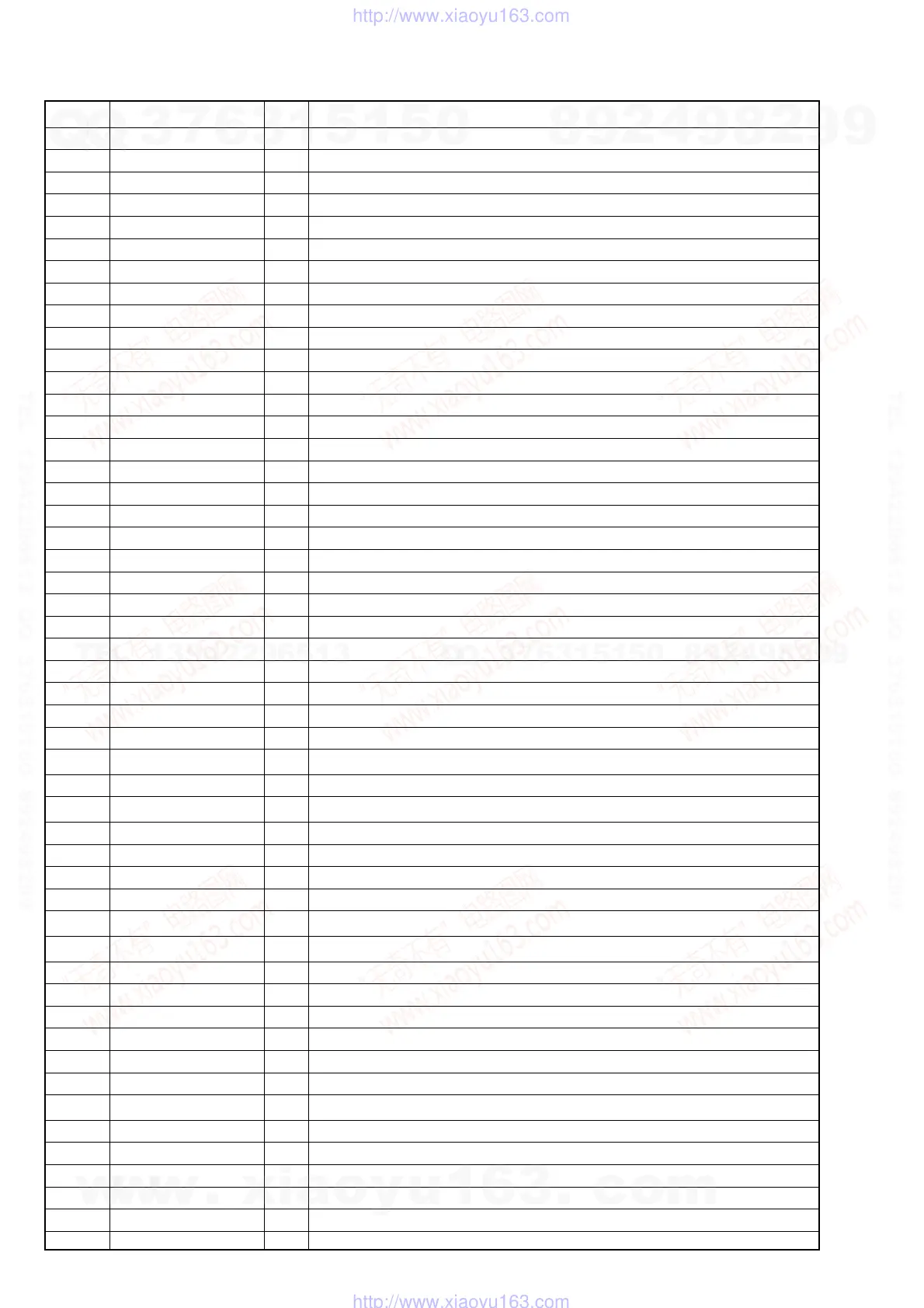
56
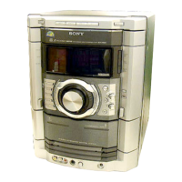
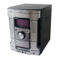
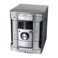
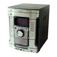
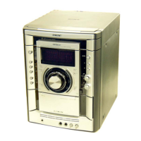
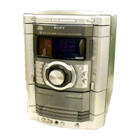
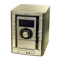
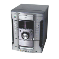
HCD-GN660/GN770/GX9000
Pin No. Pin Name I/O Description
51 A-PLAY I TCM-A play switch input
52 A-TRIG O TCM-A trigger output
53 A-HALF I A deck half detection signal input
54 CAPM-CONT O Capstan motor REV/FWD/STOP control signal output
55 REC (FWD) O Record tab switch for SIDE A signal output
56 B-PLAY I TCM-B play switch input
57 B-TRIG O TCM-B Trigger output
58 REC (REV) O Record tab switch for SIDE B signal output
59 TC-RELAY O REC/PB selection signal output
60 REC BIAS O Bias on/off signal output
61 AMS-IN I AMS signal input
62 VCC — Power supply (+3.3V)
63 TC-MUTE O TC line mute signal output
64 VSS — Ground
65 AUDIO1-DATA O Serial data output to Audio EQIC
66 AUDIO1-CLK O Serial data clock output to Audio EQIC
67 AUDIO2-DATA O Serial data output to Audio EQIC (not used)
68 AUDIO2-CLK O Serial data clock output to Audio EQIC (not used)
69 AC-CUT-MAIN I AC cut check signal input
70 STBY-RELEY O Reley drive signal output
71 CTR-RLY O Not used
72 REAR SW-RELAY O Subwoofer relay control signal output
73 DISPLAY-KEY I DISPLAY key signal input
74 POWER-KEY I Power key signal input
75 GC-RESET O GC reset signal output
76 STBY-LED O Standby LED drive signal output
77 LINK-RLY O Surround speaker relay driver signal output
78 FR-RELAY O Front speaker relay driver signal output
––––––––––––––––––
79 HP-MUTE O Headphone mute signal output
80 STK-MUTE O Mute signal output to power IC
––––––––––
81 PROT I Speaker protection signal input
82 ST-CLK O Tuner clock signal output
83 ST-DIN I Tuner data input
84 ST-DOUT O Tuner data output
85 ST-CE O Tuner chip enable signal output
––––––––––––––
86 TUNED I Tuned signal input
–––––––––––––––
87 STEREO I Stereo signal input
88 ST-MUTE O Tuner mute signal output
89 A-PHOTO OUT I TCM-A reel pulse input
90 B-PHOTO OUT I TCM-B reel pulse input
91 B-HALF I B deck half detection input
92 MODEL-IN I Model input
93 DEST-IN I Destination input
––––––––––––––––––––––––––
94 THER MAL VACS IN I VACS signal input
95
DVD-PWR-CHK/SW AO KEY
I Subwoofer ON/OFF and SURROUND SPEAKER MODE key input (not used)
96 AVSS — Ground
97 FUSELESS SW I Over-voltage protection detection input termnal
98 VREF I Reference voltage input
99 AVCC — Power supply (+3.3V)
100 XTCN/MIC DET O Oscillation circuit control signal output
w
w
w
.
x
i
a
o
y
u
1
6
3
.
c
o
m
Q
Q
3
7
6
3
1
5
1
5
0
9
9
2
8
9
4
2
9
8
T
E
L
1
3
9
4
2
2
9
6
5
1
3
9
9
2
8
9
4
2
9
8
0
5
1
5
1
3
6
7
3
Q
Q
TEL 13942296513 QQ 376315150 892498299
TEL 13942296513 QQ 376315150 892498299
http://www.xiaoyu163.com
http://www.xiaoyu163.com