98
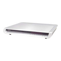
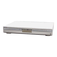
HCD-SR4W
Pin No. Pin Name I/O Description
62 PHREFO O Bit clock signal (2.8224 MHz) output to the digital audio processor Not used
63 ZDFL O Front L-ch Zero data flag detection signal output terminal Not used
64 DSAL O Front L-ch DSD data output to the digital audio processor
65 ZDFR O Front R-ch Zero data flag detection signal output terminal Not used
66 DSAR O Front R-ch DSD data output to the digital audio processor
67 VDDSD0 — Power supply terminal (+3.3V) (for DSD data output)
68 ZDFC O Center zero data flag detection signal output terminal Not used
69 DSAC O Center DSD data output to the digital audio processor
70 ZDFLFE O Woofer zero data flag detection signal output terminal Not used
71 DSALFE O Woofer DSD data output to the digital audio processor
72 VSDSD1 — Ground terminal (for DSD data output)
73 ZDFLS O Rear L-ch zero data flag detection signal output terminal Not used
74 DSALS O Rear L-ch DSD data output to the digital audio processor
75 ZDFRS O Rear R-ch zero data flag detection signal output terminal Not used
76 DSARS O Rear R-ch DSD data output to the digital audio processor
77 VDDSD — Power supply terminal (+3.3V) (For DSD data output)
78, 79 IOUT0, IOUT1 O Data output terminal for IEEE 1394 link chip interface Not used
80 VSCB0 — Ground terminal (for core)
81, 82 IOUT2, IOUT3 O Data output terminal for IEEE 1394 link chip interface Not used
83 VDCB0 — Power supply terminal (+2.5V) (for core)
84, 85 IOUT4, IOUT5 O Data output terminal for IEEE 1394 link chip interface Not used
86 VSIOB0 — Ground terminal (for I/O)
87 IANCO O
Transmission information data output terminal for IEEE 1394 link chip interface
Not used
88 IFULL I
Data transmission hold request signal input terminal for IEEE 1394 link chip
interface Not used
89 IEMPTY I
High speed transmission request signal input terminal for IEEE 1394 link chip
interface Not used
90 VDIOB0 — Power supply terminal (+3.3V) (for I/O)
91 IFRM O Frame reference signal output terminal for IEEE 1394 link chip interface Not used
92 IOUTE O Enable signal output terminal for IEEE 1394 link chip interface Not used
93 IBCK O
Data transmission clock signal output terminal for IEEE 1394 link chip interface
Not used
94 VSCB1 — Ground terminal (for core)
95 IERR I Not used
96 IANCI I Not used
97 IPLAN I Not used
98 IHOLD O Not used
99 VDCB1 — Power supply terminal (+2.5V) (for core)
100 IVLD I Not used
101 to 105 IDIN0 to IDIN4 I Not used
106 VSIOB1 — Ground terminal (for I/O)
107 to 109 IDIN5 to IDIN7 I Not used
110 VDIOB1 — Power supply terminal (+3.3V) (for I/O)
111 to 114 WAD0 to WAD3 I External A/D data input terminal for PSP physical disc mark detection Not used
115 TESTI I Input terminal for the test (normally: fixed at “L”)
116 VSCB2 — Ground terminal (for core)
w
w
w
.
x
i
a
o
y
u
1
6
3
.
c
o
m
Q
Q
3
7
6
3
1
5
1
5
0
9
9
2
8
9
4
2
9
8
T
E
L
1
3
9
4
2
2
9
6
5
1
3
9
9
2
8
9
4
2
9
8
0
5
1
5
1
3
6
7
3
Q
Q
TEL 13942296513 QQ 376315150 892498299
TEL 13942296513 QQ 376315150 892498299
http://www.xiaoyu163.com
http://www.xiaoyu163.com