19
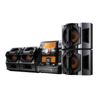
HCD-VX555/VX555J
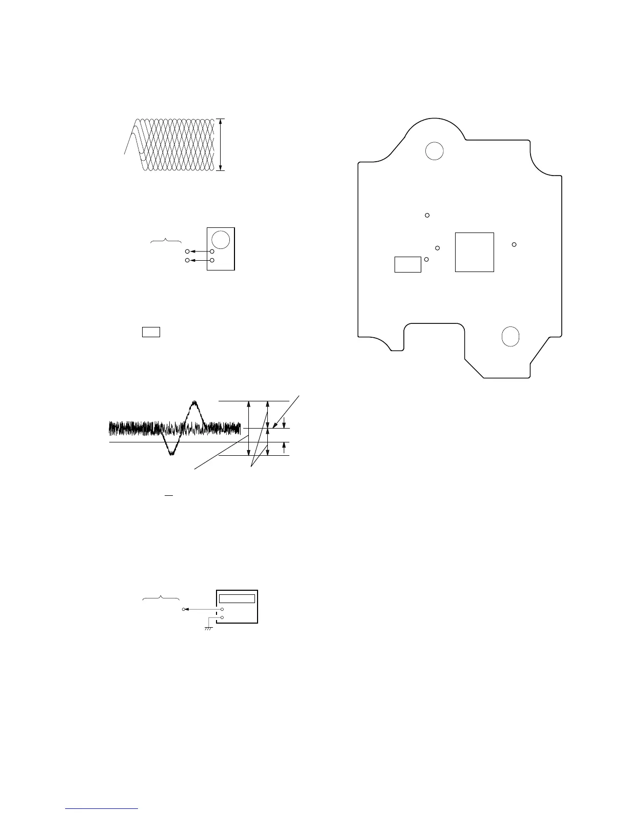
Note: Clear RF signal waveform means that the shape “◊” can be
clearly distinguished at the center of the waveform.
RF signal waveform
E-F Balance (1 Track jump) Check
Procedure:
1. Connect oscilloscope to TP (TEO) and TP (DVC) board.
2. Turned Power switch on.
3. Load a disc (YEDS-18) and playback the number five track.
4. Press the u button. (Becomes the 1track jump mode.)
5. Confirm that the level B and A (DC voltage) on the oscilloscope
waveform.
1 track jump waveform
Specification level: x 100=less than ±22%
6. After check, remove the lead wire connected in step 1.
RF PLL Free-run Frequency
Procedure :
1. Connect frequency counter to test point (XPCK) with lead wire.
2. Turned Power switch on.
3. Put the disc (YEDS-18) in to play the number five track.
Confirm that reading on frequency counter is 4.3218MHz.
oscilloscope
BD board
TP (TEO)
TP (DVC)
+
–
A
B
+
–
frequency counte