57
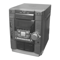
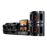
HCD-VX555/VX555J
Pin No.
52
53
54
55
56
57 to 59
60, 61
62
63
64
65
66
67 to 72
73
74
75
76
77
78
79
80
81
82
83
84
85
86
87
88
89
90 to 92
93
94
95
96
97
98
99
100
I/O
—
I
I
—
—
—
—
—
—
—
O
O
O
O
I
I
I
O
—
—
—
—
O
O
I
I
O
O
O
—
—
—
—
O
—
O
I
—
—
Description
Not used (open)
Not used (open)
Not used (open)
Not used (open)
Not used (open)
Not used (open)
Not used (open)
Power supply terminal (+5V)
Not used (open)
Ground terminal
Video muting on/off control signal output
Audio DAC reset signal output (H:Active)
Not used (open)
LED drive signal output for MPEG1 decoder test “H” (LED on)
Not used
Not used
Terminal for Test Mode 3 VCD check
System reset signal output “L”:reset
Not used (open)
Not used (open)
Not used (open)
Not used (open)
Laser power selection signal output to the CXA2581N (IC103) “H”: laser on
Sub-code Q data reading clock signal output to the CXD3068Q (IC101)
Sub-code Q data input from the CXD3068Q (IC101)
HRDY serial signal input from the CL680 (IC505)
Reset signal output to the CL680 (IC505) “L”: reset
HSEL serial signal output to the CL680 (IC505)
Serial data latch pulse output to the D/A converter (IC509) “L” active
Not used (open)
Not used (open)
Not used (open)
Not used (open)
Serial data output to the CXD3068Q (IC101)
Ground terminal (for A/D conversion)
Serial data latch pulse output to the CXD3068Q (IC101)
Reference voltage (+5V) input terminal (for A/D conversion)
Power supply terminal (+5V) (for A/D conversion)
Not used (open)
Pin Name
OUTSW
MODEL1
MODEL2
TBLL
TBLR
ENC1 to ENC3
VCC
VSS
V.MUTE
DAC RESET
A5 to A0
TEST LED
TEST1
TEST2
TEST3
DEVICE RESET
STANDBY
FL CS
FLBLK
LPH
LD ON
SUBQ CLK
SUBQ DATA
CL680 HRDY
680 RESET
CL680 HSEL
DF LATCH
MIC CTRL
KEY1 to KEY3
NT/PAL
MUSIC VOL
DSP DATA
AVSS
DSP LATCH
VREF
AVCC
AMP ON