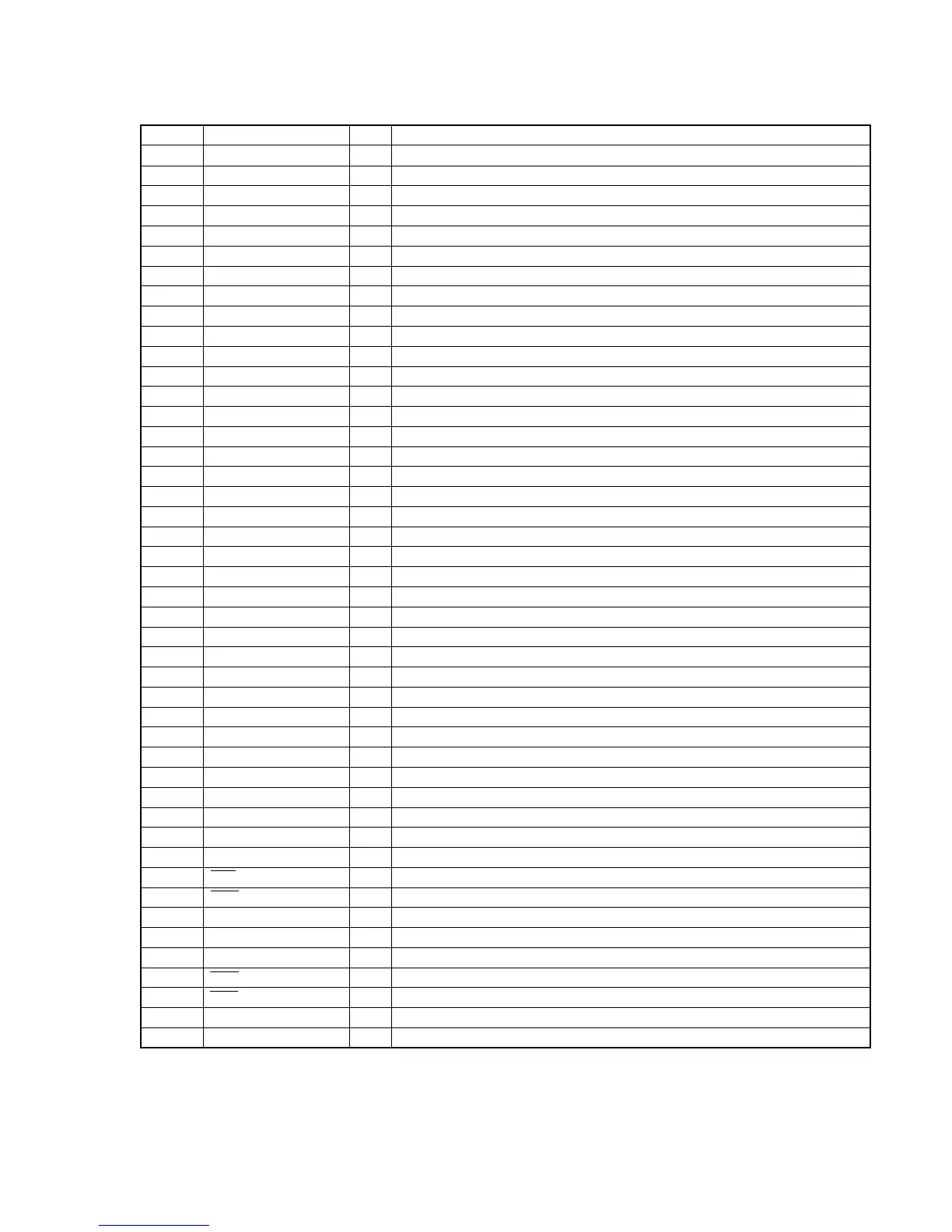
51
FunctionPin Name
1NC – Not used
2 VSS – Ground
3 CD-BCK I CD Decode bit clock
4 CD-DATA I CD Decode data
5 CD-LRCK I CD Decode Left or Right channel selection clock
6 CD-C2PO I CD Decode C2 error data
7NC – Not used
8NC – Not used
9NC – Not used
10 MD0 I/O Data bus between Microcode ROM/DRAM and CL680
11 MD1 I/O Data bus between Microcode ROM/DRAM and CL680
12 MD2 I/O Data bus between Microcode ROM/DRAM and CL680
13 MD3 I/O Data bus between Microcode ROM/DRAM and CL680
14 MD4 I/O Data bus between Microcode ROM/DRAM and CL680
15 MD5 I/O Data bus between Microcode ROM/DRAM and CL680
16 VSS – Ground
17 MD6 I/O Data bus between Microcode ROM/DRAM and CL680
18 VDD3 – +3.3V Power supply
19 MD7 I/O Data bus between Microcode ROM/DRAM and CL680
20 VSS – Ground
21 MD8 I/O Data bus between Microcode ROM/DRAM and CL680
22 VDD3 – +3.3V Power supply
23 MD9 I/O Data bus between Microcode ROM/DRAM and CL680
24 MD10 I/O Data bus between Microcode ROM/DRAM and CL680
25 MD11 I/O Data bus between Microcode ROM/DRAM and CL680
26 MD12 I/O Data bus between Microcode ROM/DRAM and CL680
27 MD13 I/O Data bus between Microcode ROM/DRAM and CL680
28 MD14 I/O Data bus between Microcode ROM/DRAM and CL680
29 MD15 I/O Data bus between Microcode ROM/DRAM and CL680
30 NC – Not used
31 NC – Not used
32 NC – Not used
33 NC – Not used
34 NC – Not used
35 NC – Not used
36 NC – Not used
37 MCE O Chip enable signal to Microcode ROM
38 MWE O Write enable signal to DRAM
39 VSS – Ground
40 CAS O Column address strove : Latch the column address to DRAM
41 VDD3 – +3.3V power supply
42 RAS0 O Row address strove : Latch row address to DRAM
43 RAS1 – Not used
44 MA10 O Address data from CL680 to Microcode ROM
45 MA9 O Address data from CL680 to Microcode ROM
Pin No. I/O
• IC505 CD DECODER, SYSTEM CONTROL (CL680T-D1) (VIDEO Board (2/3))
 Loading...