47
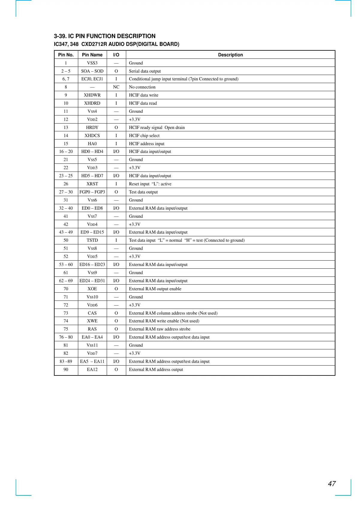
3-39. IC PIN FUNCTION DESCRIPTION
IC347, 348 CXD2712R AUDIO DSP(DIGITAL BOARD)
Pin No.
1
2 – 5
6, 7
8
9
10
11
12
13
14
15
16 – 20
21
22
23 – 25
26
27 – 30
31
32 – 40
41
42
43 – 49
50
51
52
53 – 60
61
62 – 69
70
71
72
73
74
75
76 – 80
81
82
83 –89
90
I/O
—
O
I
NC
I
I
—
—
O
I
I
I/O
—
—
I/O
I
O
—
I/O
—
—
I/O
I
—
—
I/O
—
I/O
O
—
—
O
O
O
I/O
—
—
I/O
O
Description
Ground
Serial data output
Conditional jump input terminal (7pin Connected to ground)
No connection
HCIF data write
HCIF data read
Ground
+3.3V
HCIF ready signal Open drain
HCIF chip select
HCIF address input
HCIF data input/output
Ground
+3.3V
HCIF data input/output
Reset input “L”: active
Test data output
Ground
External RAM data input/output
Ground
+3.3V
External RAM data input/output
Test data input “L” = normal “H” = test (Connected to ground)
Ground
+3.3V
External RAM data input/output
Ground
External RAM data input/output
External RAM output enable
Ground
+3.3V
External RAM column address strobe (Not used)
External RAM write enable (Not used)
External RAM raw address strobe
External RAM address output/test data input
Ground
+3.3V
External RAM address output/test data input
External RAM address output
Pin Name
VSS3
SOA – SOD
ECJ0, ECJ1
—
XHDWR
XHDRD
VSS4
VDD2
HRDY
XHDCS
HA0
HD0 – HD4
VSS5
VDD3
HD5 – HD7
XRST
FGP0 – FGP3
VSS6
ED0 – ED8
VSS7
VDD4
ED9 – ED15
TSTD
VSS8
VDD5
ED16 – ED23
VSS9
ED24 – ED31
XOE
VSS10
VDD6
CAS
XWE
RAS
EA0 – EA4
VSS11
VDD7
EA5 – EA11
EA12