18
STR-DA4ES/DA7ES/VA333ES
SECTION 6
DIAGRAMS
6-1. IC PIN FUNCTION
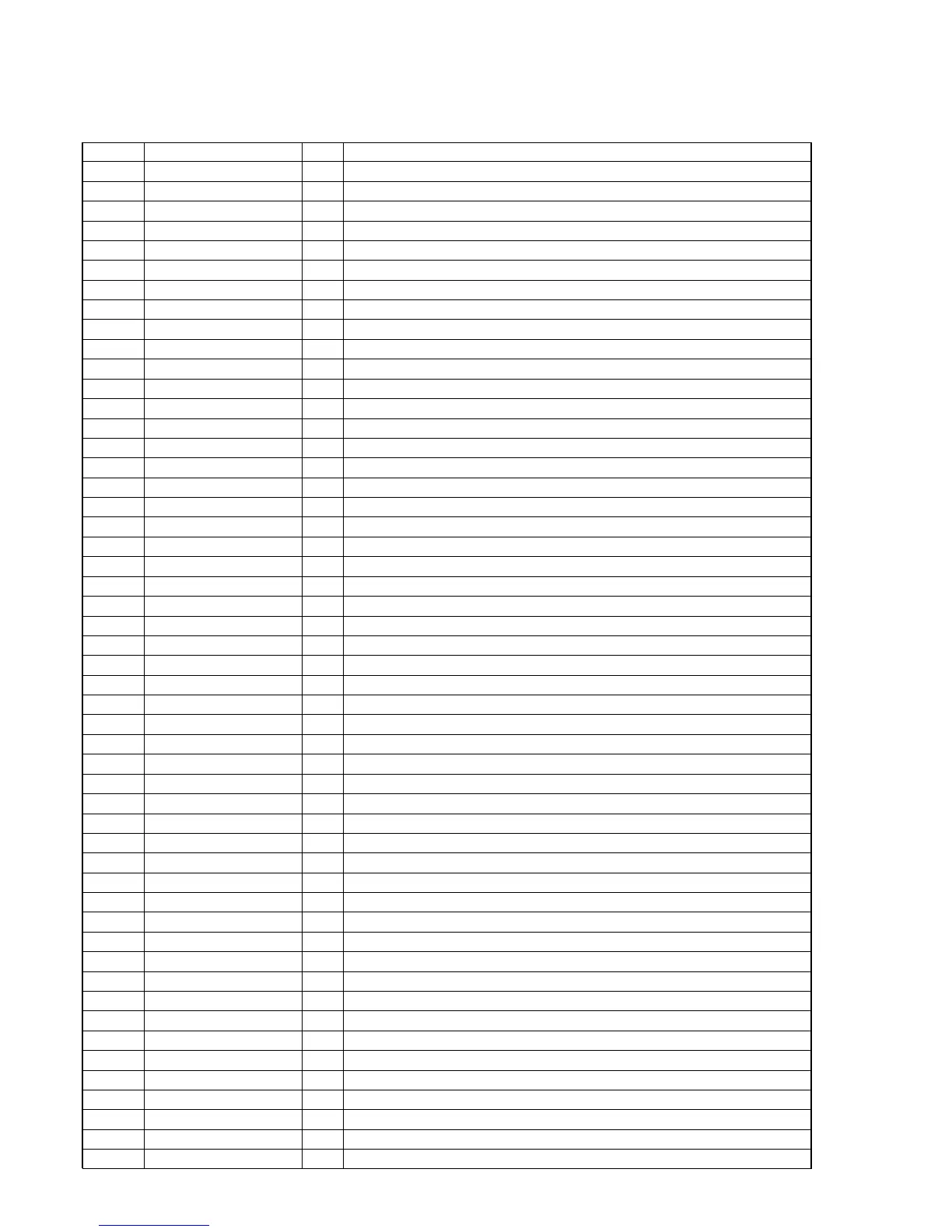
• IC1201 CXD9617R (AUDIO DSP) (DIGITAL BOARD (4/7))
Pin No. Pin Name I/O Pin Description
1 VSS — Ground pin
2 XRST I Reset signal input
3 EXTIN I Not used. (connected to ground.) Master clock signal input
4 FS2 I Not used. (connected to ground.)
5 VDDI — Power supply pin (+3.3 V)
6 FS1 I Not used. (connected to ground.)
7 PLOCK O Not used. (open)
8 VSS — Ground pin
9 MCLK1 I External crystal signal input (13.5 MHz)
10 VDDI — Power supply pin (+3.3 V)
11 VSS — Ground pin
12 MCLK2 O External crystal signal output (13.5 MHz)
13 MS I Not used. (connected to ground.)
14 SCKOUT O Not used. (open) Audio clock signal output
15 LRCKI1 I LRCK clock signal input
16 VDDE — Power supply pin (+3.3 V)
17 BCKI1 I BCK clock signal input
18 SDI1 I Audio serial data signal input
19 LRCKO O LRCK clock signal output
20 BCKO O BCK clock signal output
21 VSS — Ground pin
22 KFSIO I KFSIO signal input
23 SDO1 O Audio serial data signal output 1
24 SDO2 O Audio serial data signal output 2
25 SDO3 O Audio serial data signal output 3
26 SDO4 O Audio serial data signal output 4
27 SPDIF O Not used. (open) S/P DIF signal output
28 LRCKI2 I LRCK clock signal input
29 BCKI2 I BCK clock signal input
30 SDI2 I Audio serial data signal input
31 VSS — Ground pin
32 HACN O Host I/F acknowledge signal output
33 HDIN I Host I/F serial data signal input
34 HCLK I Host I/F serial clock signal input
35 HDOUT O Host I/F serial data signal output
36 HCS I Host I/F chip select signal input
37 SDCLK O Not used. (open)
38 CLKEN O Not used. (open)
39 RAS O Not used. (open)
40 VDDI — Power supply pin (+3.3 V)
41 VSS — Ground pin
42 CAS O Not used. (open)
43 DQM/OE0 O Not used. (open)
44 CS0 — Ground pin
45 WE0 O External memory write enable signal output
46 VDDE — Power supply pin (+3.3 V)
47 WMD1 I Not used. (connected to VDDE.) External memory wait mode signal input 1
48 VSS — Ground pin
49 WMD0 I Not used. (connected to VDDE.) External memory wait mode signal input 0
50 PAGE2 O External memory page select signal output
51 VSS — Ground pin