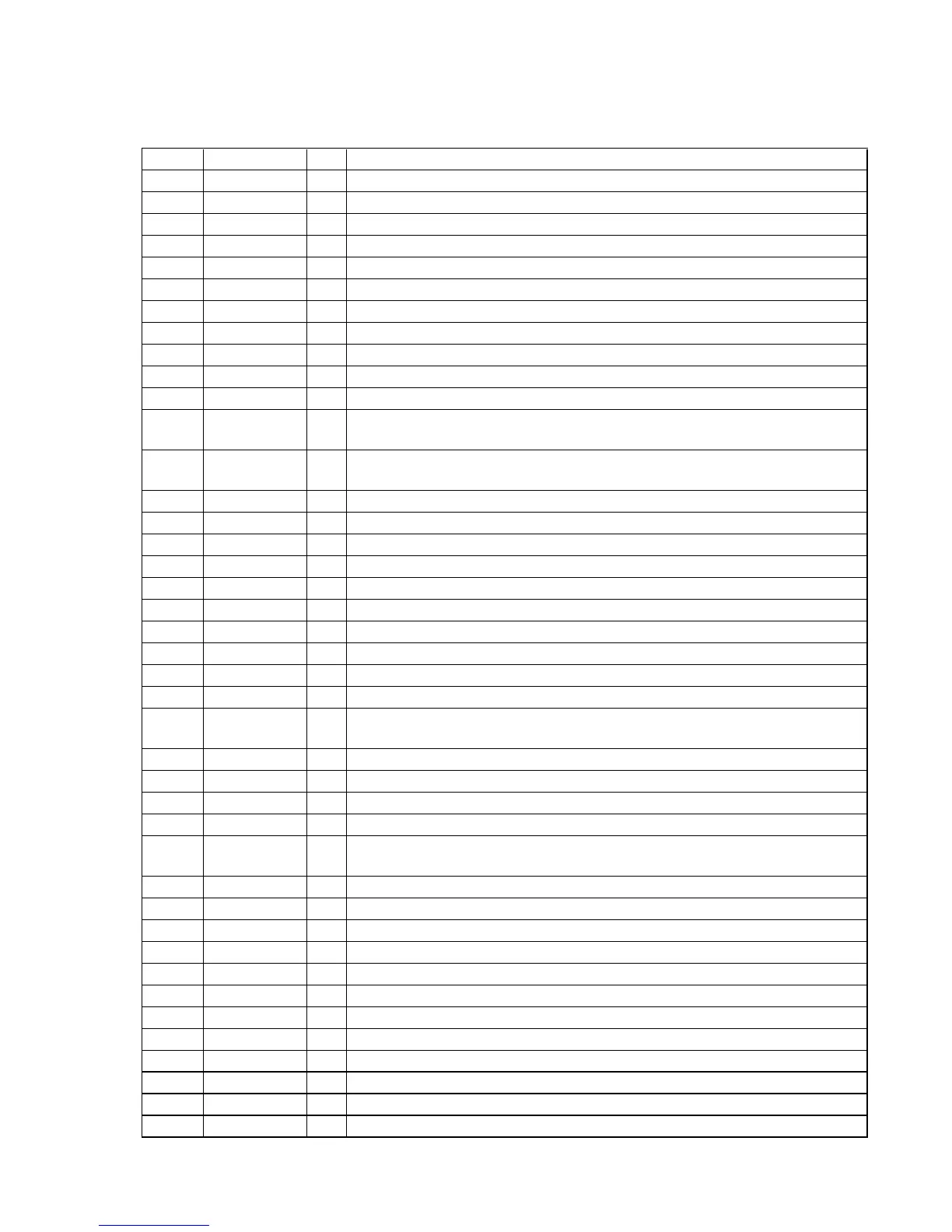
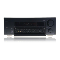
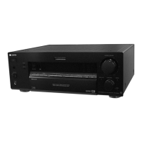
61
STR-DB798
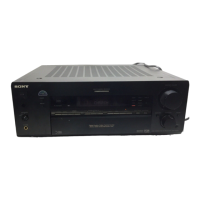
• IC Pin Function Description
DIGITAL BOARD IC1101 LC89056W-E (DIGITAL AUDIO INTERFACE RECEIVER)
Pin No.
DISEL
I
Selection signal input terminal of data input terminal Fixed at "L" in this set
DOUT
O
Digital data output to the digital optical transceiver
DIN0 to DIN2
I
Digital data input from the digital optical receiver and external input terminal
D.GND
-
Ground terminal (for digital)
DVDD
-
Power supply terminal (+3.3V) (for digital)
R
I
Input terminal for VCO gain control
VIN
I
Input terminal for VCO free-run frequency setting
LPF
O
PLL loop filter setting terminal
AVDD
-
Power supply terminal (+3.3V) (for analog)
AGND
-
Ground terminal (for analog)
CKOUT
O
Audio clock signal output to the audio digital signal processor and D/A converter
BCK
O
Bit clock signal (2.8224 MHz) output to the audio digital signal processor and A/D converter
LRCK
O
L/R sampling clock signal (44.1 kHz) output to the audio digital signal processor and A/D
converter
DATAO
O
Audio serial data output to the audio digital signal processor and system controller
XSTATE
O
Source clock selection monitor output to the system controller
DGND
-
Ground terminal (for digital)
DVDD
-
Power supply terminal (+3.3V) (for digital)
XMCK
O
System clock signal (12.288 MHz) output to the A/D converter
XOUT
O
System clock output terminal (12.288 MHz)
XIN
I
System clock input terminal (12.288 MHz)
EMPHA
O
Channel status emphasis information output terminal Not used
AUDIO
O
Channel status bit 1 output to the audio digital signal processor
CSFLAG
O
Channel status head 40 bit renewal flag output terminal Not used
Output terminal of input frequency calculation result Not used
DVDD
-
Power supply terminal (+3.3V) (for digital)
DGND
-
Ground terminal (for digital)
BPSYNC
O
Non-PCM burst preamble sync signal output terminal Not used
ERROR
O
PLL lock error signal and data error flag output to the audio digital signal processor and system
controller
DO
O
Read data output to the system controller
DI
I
Write data input from the system controller
CE
I
Chip enable signal input from the system controller
CLK
I
Clock signal input from the system controller
XSEL
I
Selection signal input terminal of crystal oscillator frequency Fixed at "H" in this set
MODE0, MODE1
I
Mode setting terminal Fixed at "L" in this set
DGND
-
Ground terminal (for digital)
DVDD
-
Power supply terminal (+3.3V) (for digital)
DOSEL0, DOSEL1
I
Output data format selection signal input terminal Fixed at "L" in this set
CKSEL0
I
Output clock selection signal input terminal Fixed at "L" in this set
CKSEL1
I
Output clock selection signal input from the system controller
XMODE
I
System reset signal input from the system controller "L": reset