Reset control AN3029
14/42 DocID16139 Rev 5
5 Reset control
5.1 Reset management overview
The reset pin is a 3.3 V bidirectional I/O. After startup it can be programmed by software to
be used as a general purpose I/O.
Its output buffer driving capability is fixed to Iol
MIN
= 2 mA @ 0.45 V in the 1.8 V to 3.6 V
range which includes a ~45 k pull-up. Output buffer is reduced to the n-channel MOSFET
(NMOS). The receiver includes a glitch filter, whereas the output buffer includes a 20 µs
delay.
There are many reset sources, including:
• External reset through the NRST pin
• Power-on reset (POR) and brown-out reset (BOR): During power-on, the POR keeps
the device under reset until the supply voltage (V
DD
and V
DDx
) reach the voltage level
at which level the BOR starts to function. STM8L101xx devices have only a POR.
• Independent watchdog reset (IWDG)
• Window watchdog reset (WWDG), featuring also software reset: only for STM8L05xx,
STM8L15xxx, STM8L162xx, STM8AL31xx, and STM8AL3Lxx.
• SWIM reset: An external device connected to the SWIM interface can request the
SWIM block to generate a microcontroller reset.
• Illegal opcode reset: If a code to be executed does not correspond to any opcode or
prebyte value, a reset is generated.
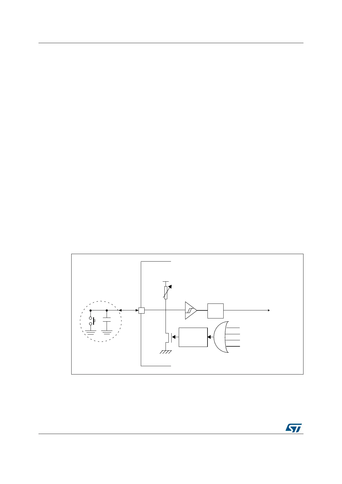
Figure 7 shows a simplified functional I/O reset schematic.
Figure 7. Reset management
R
PU
System reset
Filter
100 nF
External
reset circuit
NRST
ai14866d
Illegal op code reset
Swim reset
POR/BOR reset
IWDG/WWDG/software reset
Delay
STM8
VDD_IO
Pulse
generator
(min 20 μs)