Power supply AN3029
8/42 DocID16139 Rev 5
2.3 Power-on/power-down reset (POR/PDR)
The input supply to the main and low power regulators is monitored by a power-on/power-
down reset circuit. The monitoring voltage begins at 0.7 V.
During power-on, the POR/PDR keeps the device under reset until the supply voltages (V
DD
and V
DDA
) reach their specified working area. Maximum power on time t
VDD[max]
must be
respected, as the internal reset provided for supply stabilization is maintained for ~1
ms.
At power-on, a defined reset should be maintained below 0.7 V. The upper threshold for a
reset release is defined in the electrical characteristics section of the product datasheets.
A hysteresis is implemented (POR > PDR) to ensure clean detection of voltage rise and fall.
The POR/PDR also generates a reset when the supply voltage drops below the V
PDR
threshold (isolated and repetitive events).
Correct device reset during power-on sequence is guaranteed when t
VDD[max]
is respected.
It is recommended to use an internal BOR or an external reset circuit (especially for
STM8L101xx devices) to ensure correct device reset during power-down when V
PDR
< V
DD
< V
DD[min]
.
For better power monitoring, the STM8L15xxx, STM8L162xx, STM8AL31xx, and
STM8AL3Lxx provide a brown out reset (BOR) and programmable power voltage detection
(PVD) for an earlier detection of voltage drop.
Recommendations
All pins need to be properly connected to the power supplies. These connections, including
pads, tracks and vias should have the lowest possible impedance. This is typically achieved
with thick track widths and preferably dedicated power supply planes in multi-layer printed
circuit boards (PCBs).
In addition, each power supply pair should be decoupled with filtering ceramic capacitors (C)
at 100 nF with one chemical C (1..2 µF) in parallel on the STM8L/STM8AL devices. The
ceramic capacitors should be placed as close as possible to the appropriate pins, or below
the appropriate pins, on the opposite side of the PCB. Typical values are 10 nF to 100 nF,
but exact values depend on the application needs.
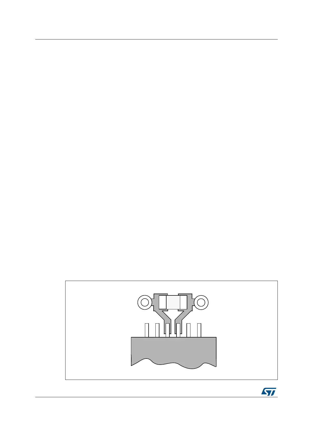
Figure 2 shows the typical layout of such
a V
DD
/V
SS
pair.
Figure 2. Typical layout of V
DD
/V
SS
pair
MS32523V1
Via to V
SS
Via to V
DD
Cap.
V
DD
V
SS
STM8