DocID16139 Rev 5 7/42
AN3029 Power supply
41
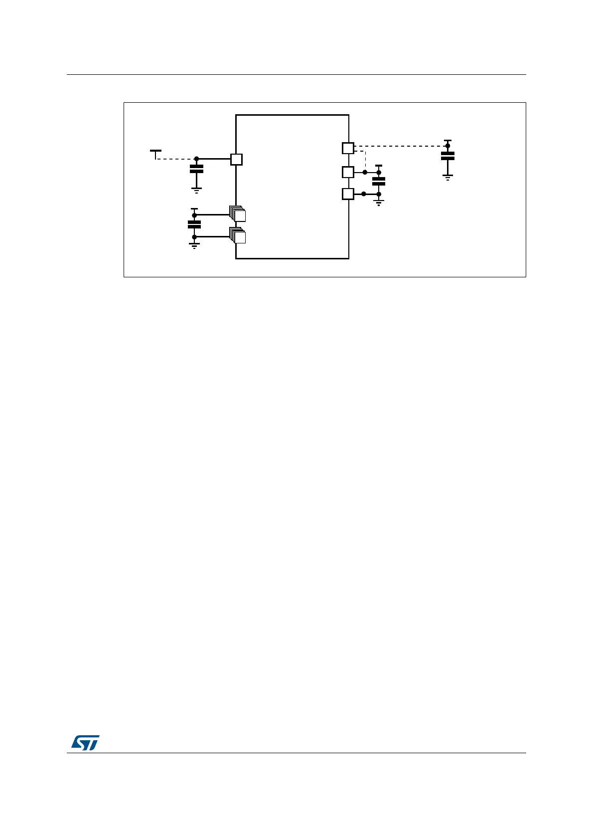
Figure 1. Power supply
1. Optional: if a separate, external reference voltage is connected on V
REF+
, the two capacitors (100 nF and 1
µF) must be connected. V
REF+
is either connected to V
DDA
or V
REF.
2. N is the number of V
DD
and V
SS
inputs.
Note: The capacitors must be connected as close as possible to the device supplies.
Placing a crystal/resonator on OSCIN/OSCOUT is optional. The resonator must be
connected as close as possible to the OSCIN and OSCOUT pins. The loading capacitance
ground must be connected as close as possible to V
SS
.
2.2 Main operating voltages
STM8L and STM8AL devices are processed in 0.13 µm technology. The STM8L and
STM8AL core and I/O peripherals need different power supplies. In fact, STM8L and
STM8AL devices have an internal regulator with a nominal target output of 1.8 V.
MS30982V1
V
LCD
STM8L/STM8AL
N × 100 nF
V
DD
+ 1 × 10 μF
100 nF + 1 μF
100 nF + 1 μF
(note 1)
V
LCD
V
REF+
V
DDA
V
SSA
V
DD 1/2/... /N
V
SS 1/2/... /N
V
REF
V
DD
1 μF
(optional)
(note 2)
(note 2)