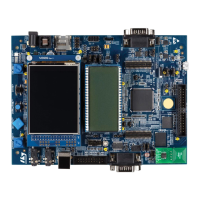
Hardware layout and configuration UM1855
18/100 DocID027351 Rev 3
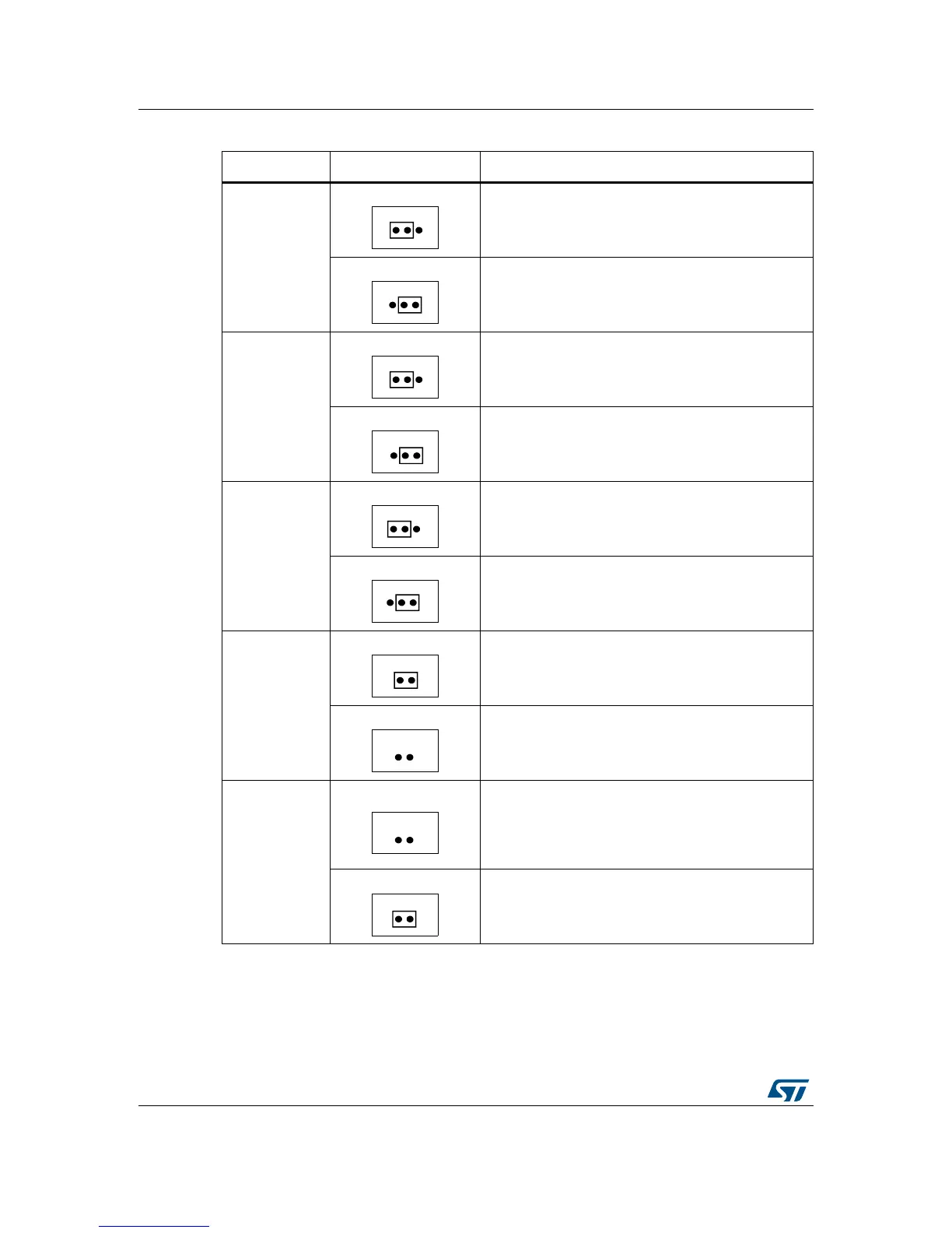
JP2
VDD_MCU
connection
JP2
Default setting.
VDD_MCU (VDD terminals of STM32L476ZGT6) is
connected to fixed +3.3 V.
JP2
VDD_MCU is connected to voltage in the range from
+1.71 V to +3.6 V, adjustable with potentiometer RV1.
JP10
VDDA
connection
JP10
Default setting.
VDDA terminal of STM32L476ZGT6 is connected with
VDD_MCU.
JP10
VDDA terminal of STM32L476ZGT6 is connected to
+3.3 V.
JP1
VDD_USB
connection
JP1
Default setting.
VDD_USB (VDDUSB terminal of STM32L476ZGT6) is
connected with VDD_MCU.
JP1
VDD_USB
is connected to +3.3V.
JP3
VDD_IO
connection
JP3
Default setting.
VDD_IO
(VDDIO2 terminals of STM32L476ZGT6) is
connected with VDD_MCU
JP3
VDD_IO
is open.
JP18
Powering
through USB of
ST-LINK/V2-1
JP18
Default setting.
Standard-B USB connector CN17 of ST-LINK/V2-1 can
supply power to the STM32L476G-EVAL board
remainder, depending on host PC USB port’s powering
capability declared in the enumeration.
JP18
Standard-B USB connector CN17 of ST-LINK/V2-1
supplies power to the STM32L476G-EVAL board
remainder. Setting for powering the board through
CN17 using USB charger.
Table 2. Power-supply-related jumper settings (continued)
Jumper array Jumper setting Configuration