EasyManua.ls Logo

STMicroelectronics STM32L476G-EVAL User Manual

STMicroelectronics STM32L476G-EVAL
100 pages
To Next Page IconTo Next Page
To Previous Page IconTo Previous Page
Page #55 background image
DocID027351 Rev 3 55/100
UM1855 Hardware layout and configuration
99
that communicate with the MCU through I/O ports. Voltage exceeding 3.3 V on the MCU
output port may inject current into 3.3 V-supplied peripheral I/Os and false the MCU current
consumption measurement.
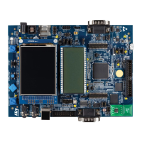
2.30.1 IDD measurement principle - analog part
The analog part is based on measuring voltage drop across a shunt resistor, amplified with a
differential amplifier. The STM32L476ZGT6 microcontroller supply current is shunted, by
jumper settings, to flow through the measurement 1 resistor R135: JP11 terminals 1 and 2
are to be open, terminals 3 and 4 closed. When the transistor T2 is in conductive state, the
MCU supply current is proportional to the voltage across R135. When T2 is in high-
impedance state, the MCU supply current is proportional to the voltage across the series of
R135 and R123. The former state is used for measuring the current consumption in dynamic
run mode, the latter in low-power mode.
The differential amplifier uses three stages U15B, U15C, U15D of quadruple operational
amplifier device U15, TSZ124. The gain is set to 50, so every 1 mA of supply current is
represented by additional 50 mV at the U15C output, terminal 8 of U15.
The resistance formed with the series of R135 and R123, when T2 is in high-impedance
state, is of 1001 . It makes the voltage on terminal 8 of U15 increase by approximately
50 mV for every µA of MCU power consumption. The full-scale range, with VDD at 1.8 V is
about 30 µA.
Even with precision resistors R136, R125, R129, R132 to set the gain of the differential
amplifier, the output voltage may theoretically become negative. To avoid the need of
negative power supply, a positive offset of about 220 mV is created at the output, at zero
current consumption of the MCU. This offset does not need to be precise. Any dispersion is
compensated through a calibration procedure detailed in Section 2.30.4.
For allowing the IDD measurement, the jumper in the JP11 header must be placed such as
to short its terminals 3 and 4.

Table of Contents

Question and Answer IconNeed help?

Do you have a question about the STMicroelectronics STM32L476G-EVAL and is the answer not in the manual?

STMicroelectronics STM32L476G-EVAL Specifications

General IconGeneral
CoreARM Cortex-M4
Flash Memory1 MB
SRAM128 KB
Operating Voltage1.71 V to 3.6 V
Clock Speed80 MHz
On-Board DebuggerST-LINK/V2-1
EEPROMNo
Debug InterfaceSWD
USBUSB 2.0
Development EnvironmentSTM32CubeIDE
ConnectorsUSB, Audio jack
ADC12-bit ADC
DAC12-bit DAC
Communication InterfacesI2C, SPI, USART, USB, CAN
Operating Temperature-40°C to +85°C
Power ConsumptionLow power consumption

Summary

Introduction to STM32L476G-EVAL Board

Overview of STM32L476G-EVAL

Features of the STM32L476G-EVAL Board

Detailed list of hardware and software features of the evaluation board.

Demonstration Software

Information on the preloaded demonstration software for easy peripheral evaluation.

Order Code

Procedure to order the STM32L476G-EVAL board.

Unpacking Recommendations

Instructions for safe unpacking and checking components of the evaluation board.

Hardware Layout and Configuration

ST-LINK/V2-1 Debug and Flashing

Details on the integrated ST-LINK/V2-1 debugger and flashing tool.

Power Supply Options

Methods and configurations for powering the evaluation board.

Microcontroller Boot Options

Configuration options for the microcontroller's boot process.

USB OTG FS Port Functionality

Functionality and configuration of the USB OTG Full-Speed port.

microSD Card Interface

Interface and operation of the microSD card slot.

Motor Control Interface

Interface and configuration for motor control modules.

Current Consumption Measurement

Onboard circuit for measuring MCU current consumption.

Touch-Sensing Button

Functionality and configuration of the touch-sensing button.

Smartcard and SWP Interface

Interface and operation for smartcards and SWP.

Connectors and Interfaces

RS-232 D-sub Male Connector CN9

Pin assignment and details for the RS-232 connector.

Power Connector CN22

Details of the external power supply connector.

Extension Connectors CN6 and CN7

Headers for daughterboard expansion and GPIO access.

ST-LINK/V2-1 USB Connector CN17

USB connector for ST-LINK/V2-1 functionality.

JTAG Connector CN15

Connector for JTAG debugging interface.

ETM Trace Debugging Connector CN12

Connector for ETM trace debugging.

microSD Card Connector CN18

Connector for interfacing with microSD cards.

Motor Control Connector CN2

Connector for connecting motor control modules.

USB OTG FS Micro-AB Connector CN1

Connector for USB OTG Full-Speed interface.

Appendix A: Schematic Diagrams

STM32L476G-EVAL Top Schematic

Top-level schematic diagram of the evaluation board.

Power Supply Schematic Diagram

Schematic diagram of the board's power supply circuitry.

SRAM and NOR Flash Memory Schematic

Schematic diagram for SRAM and NOR Flash memory.

IDD Measurement Schematic Diagram

Schematic diagram for MCU current consumption measurement.

Appendix B: Compliance Statements

FCC Compliance Statement

Statement regarding compliance with FCC regulations.

IC Compliance Statement

Statement regarding compliance with Industry Canada regulations.

Revision History

Related product manuals