DocID027351 Rev 3 45/100
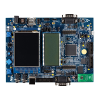
UM1855 Hardware layout and configuration
99
wired through I²C bus or wireless using 13.56 MHz RF band reserved for RFID and NFC
equipment. For wireless access, CR95HF reader daughterboard plugged in the CN13
connector can be used, for example.
I²C address of RF-EEPROM device is 0xA6.
2.25 Quad-SPI Flash memory device
N25Q256A13EF840E, a 256-Mbit Quad-SPI Flash memory device, is fitted on the
STM32L476G-EVAL main board, in U9 position. It allows evaluating STM32L476ZGT6
Quad-SPI Flash memory device interface.
N25Q256A13EF840E can operate in single transfer rate (STR) and double transfer rate
(DTR) modes.
By default, the Quad-SPI Flash memory device is not accessible. Table 26 shows the
configuration elements and their settings allowing to access the Quad-SPI Flash memory
device. The LCD glass module daughterboard MB979 takes active part in the configuration.
It must be removed from the main board (denoted as “MB979 out”), to operate the Quad-
SPI Flash memory device. Section 2.12: Motor control provides additional information.
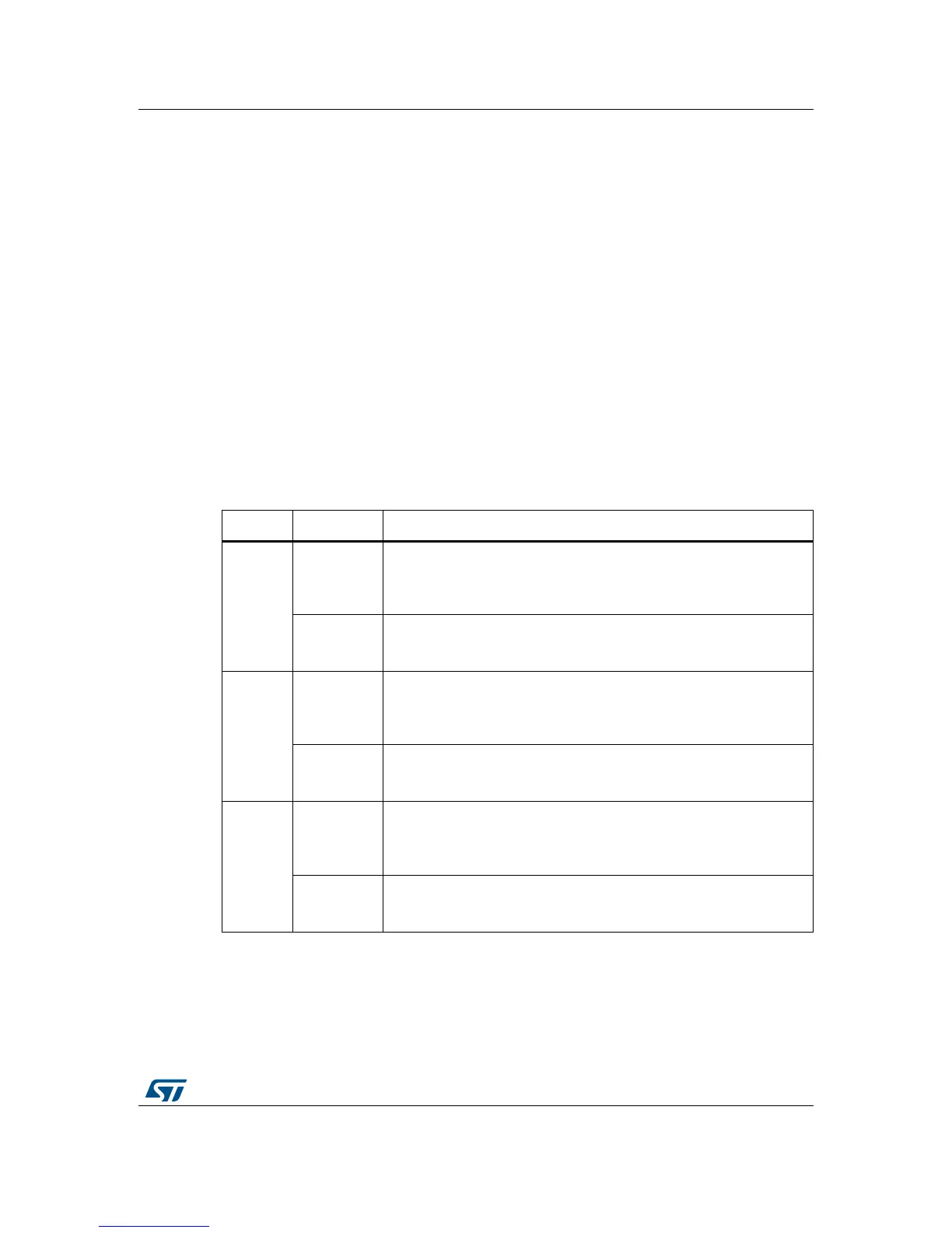
Table 26. Configuration elements related with Quad-SPI device
Element Setting Configuration
SB12
SB13
MB979
SB12 open
SB13 open
Default setting.
QSPI_D0 data line is not available at Quad-SPI Flash memory device:
PB1 port of STM32L476ZGT6 is only routed to CN11 connector for the
MB979 daughterboard.
SB12 closed
SB13 open
MB979 out
QSPI_D0 data line is available at Quad-SPI Flash memory device:
PB1 port of STM32L476ZGT6 is routed to DQ0 port of Quad-SPI Flash
memory device.
SB14
SB15
MB979
SB14 open
SB15 open
Default setting.
QSPI_D1 data line is not available at Quad-SPI Flash memory device:
PB0 port of STM32L476ZGT6 is only routed to CN11 connector for the
MB979 daughterboard.
SB14 closed
SB15 open
MB979 out
QSPI_D1 data line is available at Quad-SPI Flash memory device:
PB0 port of STM32L476ZGT6 is routed to DQ1 port of Quad-SPI Flash
memory device.
SB18
SB19
MB979
SB18 open
SB19 open
Default setting.
QSPI_D2 data line is not available at Quad-SPI Flash memory device:
PA7 port of STM32L476ZGT6 is only routed to CN11 connector for the
MB979 daughterboard.
SB18 closed
SB19 open
MB979 out
QSPI_D2 data line is available at Quad-SPI Flash memory device:
PA7 port of STM32L476ZGT6 is routed to DQ2 port of Quad-SPI Flash
memory device.