Hardware layout and configuration UM1855
36/100 DocID027351 Rev 3
corresponding to each COMx and SEGy combination. Names in quoting marks denote
elements forming textual symbols, for example “µA” or “+”. Figure 11 shows the physical
location and shape of each segment on the LCD glass module.
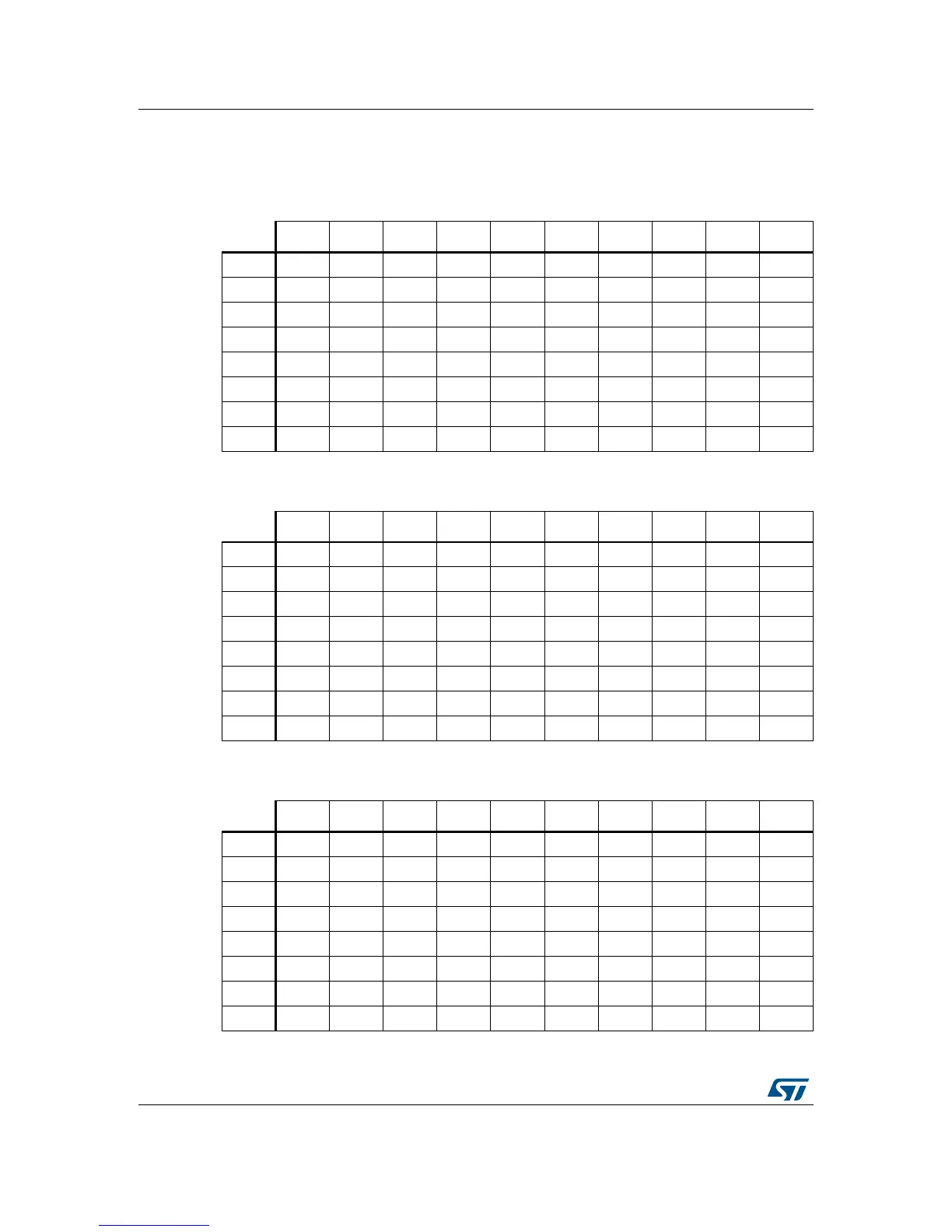
Table 15. LCD glass element mapping - segments 0 to 9
SEG0 SEG1 SEG2 SEG3 SEG4 SEG5 SEG6 SEG7 SEG8 SEG9
COM0 O1 5D Q4 O4 6D Q5 ST 7D Q6 S5
COM1 O2 5K 5L O3 6K 6L “nA” 7K 7L S6
COM2 13b 12b 11b 16b 15b 14b 19b 18b 17b 1b
COM3 13a 12a 11a 16a 15a 14a 19a 18a 17a 1a
COM4 5I 5A 5G 6I 6A 6G 7I 7A 7G 1I
COM5 5B 5H 5F 6B 6H 6F 7B 7H 7F 1B
COM6 5C 5M P4 6C 6M P5 7C 7M P6 1C
COM7 5J 5N 5E 6J 6N 6E 7J 7N 7E 1J
Table 16. LCD glass element mapping - segments 10 to 19
SEG10 SEG11 SEG12 SEG13 SEG14 SEG15 SEG16 SEG17 SEG18 SEG19
COM0 1D “-” C1 2D Q1 C4 3D Q2 “µA” 4D
COM1 1K 1L C2 2K 2L C3 3K 3L “mA” 4K
COM2 S4 S2 4b 3b 2b 7b 6b 5b 10b 9b
COM3 S3 S1 4a 3a 2a 7a 6a 5a 10a 9a
COM4 1A 1G 2I 2A 2G 3I 3A 3G 4I 4A
COM5 1H 1F 2B 2H 2F 3B 3H 3F 4B 4H
COM6 1M“+”2C2MP13C3MP24C4M
COM7 1N 1E 2J 2N 2E 3J 3N 3E 4J 4N
Table 17. LCD glass element mapping - segments 20 to 29
SEG20 SEG21 SEG22 SEG23 SEG24 SEG25 SEG26 SEG27 SEG28 SEG29
COM0 Q3 1e 2e 3e 4e 5e 6e 7e 8e 9e
COM1 4L 1f 2f 3f 4f 5f 6f 7f 8f 9f
COM2 8b 1c 2c 3c 4c 5c 6c 7c 8c 9c
COM3 8a 1d 2d 3d 4d 5d 6d 7d 8d 9d
COM4 4G 1j 2j 3j 4j 5j 6j 7j 8j 9j
COM5 4F 1i 2i 3i 4i 5i 6i 7i 8i 9i
COM6 P3 1h 2h 3h 4h 5h 6h 7h 8h 9h
COM7 4E 1g 2g 3g 4g 5g 6g 7g 8g 9g