DocID027351 Rev 3 7/100
UM1855 List of figures
8
List of figures
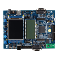
Figure 1. STM32L476G-EVAL evaluation board . . . . . . . . . . . . . . . . . . . . . . . . . . . . . . . . . . . . . . . . . 1
Figure 2. STM32L476G-EVAL hardware block diagram . . . . . . . . . . . . . . . . . . . . . . . . . . . . . . . . . . 11
Figure 3. STM32L476G-EVAL main component layout. . . . . . . . . . . . . . . . . . . . . . . . . . . . . . . . . . . 12
Figure 4. USB Composite device. . . . . . . . . . . . . . . . . . . . . . . . . . . . . . . . . . . . . . . . . . . . . . . . . . . . 13
Figure 5. CN22 power jack polarity . . . . . . . . . . . . . . . . . . . . . . . . . . . . . . . . . . . . . . . . . . . . . . . . . . 16
Figure 6. CN20, CN21 top view . . . . . . . . . . . . . . . . . . . . . . . . . . . . . . . . . . . . . . . . . . . . . . . . . . . . . 23
Figure 7. PCB top-side rework for motor control . . . . . . . . . . . . . . . . . . . . . . . . . . . . . . . . . . . . . . . . 30
Figure 8. PCB underside rework for motor control. . . . . . . . . . . . . . . . . . . . . . . . . . . . . . . . . . . . . . . 31
Figure 9. LCD glass module daughterboard in display position. . . . . . . . . . . . . . . . . . . . . . . . . . . . . 33
Figure 10. LCD glass module daughterboard in I/O-bridge position . . . . . . . . . . . . . . . . . . . . . . . . . . 34
Figure 11. LCD glass display element mapping . . . . . . . . . . . . . . . . . . . . . . . . . . . . . . . . . . . . . . . . . 38
Figure 12. NFC board plugged into STM32L476G-EVAL board . . . . . . . . . . . . . . . . . . . . . . . . . . . . . 50
Figure 13. Routing of STPMS2L dual-channel sigma-delta modulators . . . . . . . . . . . . . . . . . . . . . . . 52
Figure 14. Power measurement principle schematic diagram . . . . . . . . . . . . . . . . . . . . . . . . . . . . . . . 53
Figure 15. STPMS2L power metering schematic diagram. . . . . . . . . . . . . . . . . . . . . . . . . . . . . . . . . . 53
Figure 16. Temperature measurement principle schematic diagram. . . . . . . . . . . . . . . . . . . . . . . . . . 54
Figure 17. Schematic diagram of the analog part of IDD measurement . . . . . . . . . . . . . . . . . . . . . . . 56
Figure 18. Schematic diagram of logic part of low-power-mode IDD measurement . . . . . . . . . . . . . . 57
Figure 19. Low power mode IDD measurement timing . . . . . . . . . . . . . . . . . . . . . . . . . . . . . . . . . . . . 58
Figure 20. RS-232 D-sub (DE-9M) 9-pole connector (front view) . . . . . . . . . . . . . . . . . . . . . . . . . . . . 60
Figure 21. Power supply connector CN22 (front view) . . . . . . . . . . . . . . . . . . . . . . . . . . . . . . . . . . . . 60
Figure 22. USB type B connector CN17 (front view) . . . . . . . . . . . . . . . . . . . . . . . . . . . . . . . . . . . . . . 65
Figure 23. JTAG debugging connector CN15 (top view) . . . . . . . . . . . . . . . . . . . . . . . . . . . . . . . . . . . 66
Figure 24. Trace debugging connector CN12 (top view) . . . . . . . . . . . . . . . . . . . . . . . . . . . . . . . . . . . 67
Figure 25. microSD card connector CN18 . . . . . . . . . . . . . . . . . . . . . . . . . . . . . . . . . . . . . . . . . . . . . . 68
Figure 26. Analog input-output connector CN8 (top view) . . . . . . . . . . . . . . . . . . . . . . . . . . . . . . . . . . 68
Figure 27. RF EEPROM daughterboard connector CN3 (front view) . . . . . . . . . . . . . . . . . . . . . . . . . 69
Figure 28. Motor control connector CN2 (top view) . . . . . . . . . . . . . . . . . . . . . . . . . . . . . . . . . . . . . . . 69
Figure 29. USB OTG FS Micro-AB connector CN1 (front view). . . . . . . . . . . . . . . . . . . . . . . . . . . . . . 70
Figure 30. CAN D-sub (DE-9M) 9-pole male connector CN5 (front view) . . . . . . . . . . . . . . . . . . . . . . 71
Figure 31. NFC female connector CN13 (top view) . . . . . . . . . . . . . . . . . . . . . . . . . . . . . . . . . . . . . . . 71
Figure 32. STM32L476G-EVAL top schematic diagram . . . . . . . . . . . . . . . . . . . . . . . . . . . . . . . . . . . 73
Figure 33. MCU, LCD daughterboard and I/O expander interfaces - schematic diagram . . . . . . . . . 74
Figure 34. STM32L476G-EVAL MCU part 1 - schematic diagram . . . . . . . . . . . . . . . . . . . . . . . . . . . 75
Figure 35. STM32L476G-EVAL MCU part 2 - schematic diagram . . . . . . . . . . . . . . . . . . . . . . . . . . . 76
Figure 36. LCD glass module daughterboard connectors - schematic diagram . . . . . . . . . . . . . . . . . 77
Figure 37. I/O expander schematic diagram . . . . . . . . . . . . . . . . . . . . . . . . . . . . . . . . . . . . . . . . . . . . 78
Figure 38. Power supply schematic diagram . . . . . . . . . . . . . . . . . . . . . . . . . . . . . . . . . . . . . . . . . . . . 79
Figure 39. Smartcard, SWP and NFC - schematic diagram . . . . . . . . . . . . . . . . . . . . . . . . . . . . . . . . 80
Figure 40. USART and IrDA - schematic diagram . . . . . . . . . . . . . . . . . . . . . . . . . . . . . . . . . . . . . . . . 81
Figure 41. SRAM and NOR Flash memory devices - schematic diagram . . . . . . . . . . . . . . . . . . . . . . 82
Figure 42. TFT LCD schematic diagram . . . . . . . . . . . . . . . . . . . . . . . . . . . . . . . . . . . . . . . . . . . . . . . 83
Figure 43. Extension connector schematic diagram . . . . . . . . . . . . . . . . . . . . . . . . . . . . . . . . . . . . . . 84
Figure 44. Quad-SPI Flash memory device schematic diagram . . . . . . . . . . . . . . . . . . . . . . . . . . . . . 85
Figure 45. microSD card schematic diagram . . . . . . . . . . . . . . . . . . . . . . . . . . . . . . . . . . . . . . . . . . . 86
Figure 46. Physical control peripherals - schematic diagram. . . . . . . . . . . . . . . . . . . . . . . . . . . . . . . . 87
Figure 47. CAN transceiver schematic diagram . . . . . . . . . . . . . . . . . . . . . . . . . . . . . . . . . . . . . . . . . 88
Figure 48. Touch-sensing device schematic diagram . . . . . . . . . . . . . . . . . . . . . . . . . . . . . . . . . . . . . 89