Description
Specifications
22 X72 Desiger’s Reference and User’s Guide 097-10603-01 Rev. A – November 2004
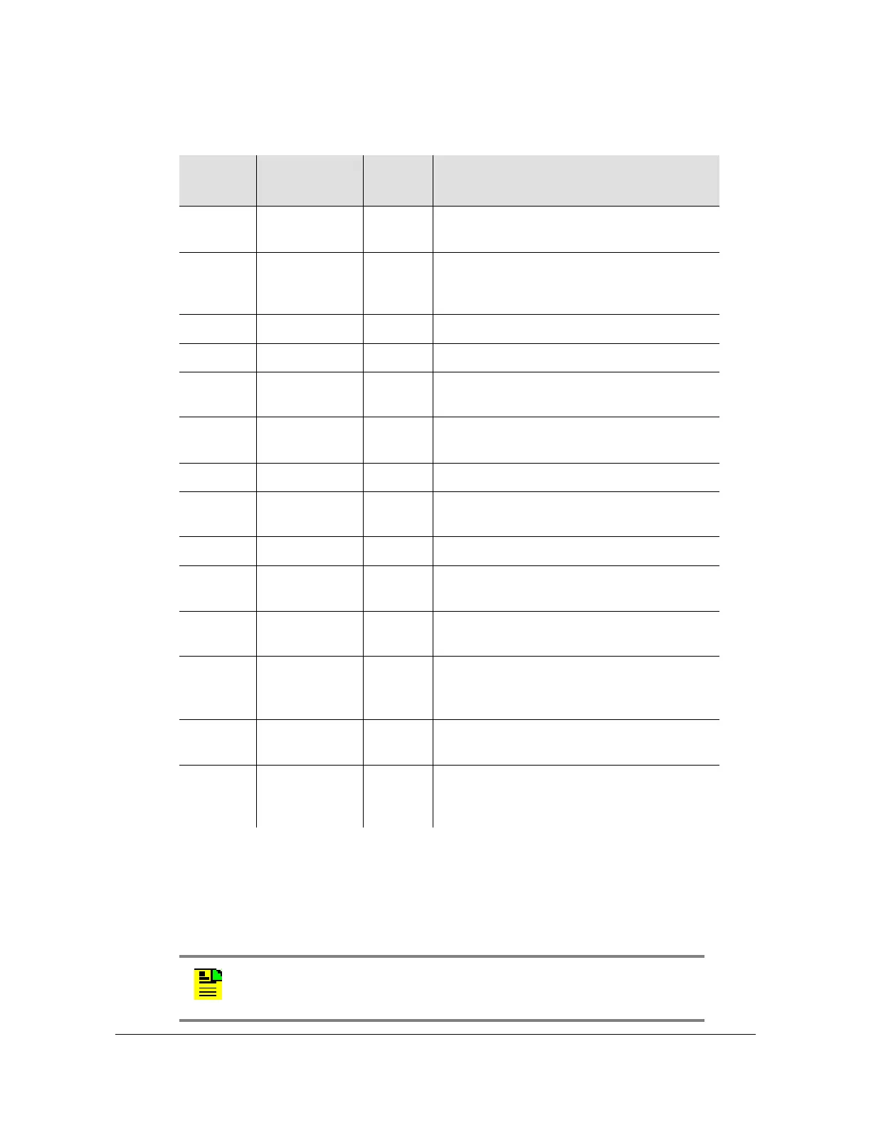
Table 1-1. X72 Design Absolute Maximum Ratings
Pin
Number
Signal Name
Type
1
Note:
1 All inputs and outputs are ESD protected, short circuit protected, and all inputs are compatible
with 3.3V ACMOS logic and 5V TTL logic.
Signal Function
1 – 7 VDD PWR + Power input +10 to +32 Vdc – all power
pins must be connected.
8 SERVICE Output Indicates unit is nearing limits of frequency
control and that Service is required within
several months.
9 DOUT Output UART data out at ACMOS logic levels.
10 DIN Input UART data in at ACMOS logic levels.
11 FREQ CTRL Analog Frequency control – analog input between
0 – 5 Vdc.
12 – 18 VSS GND – Power & signal return – all grounds must
be connected.
19 1 PPS IN Input 1 PPS input, positive edge triggered.
20 1 PPS OUT Output 1 PPS output, may be enabled/disabled
digitally.
21 LOCK Output If low, indicates Rb osc. is locked.
22 FXO
Output
2
2 High impedance
(FXO) ACMOS output equalling the VCXO
frequency.
23 FACMOS
RTN
GND Return for FACMOS & FXO signals.
24 FACMOS
OUT
Output (FACMOS) ACMOS output option - equals
VCXO frequency divided by 2xN (N is
selectable).
25 FSINE RTN GND Chassis ground – return signal for FSINE
signal.
26 FSINE OUT Output (FSINE) Sine output option – equals
VCXO frequency divided by 2xM (M is set
at the factory).
Note: Refer to Appendix A for the connector manufacturer's drawings
and specifications.
 Loading...