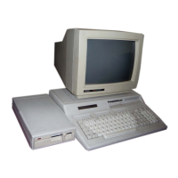
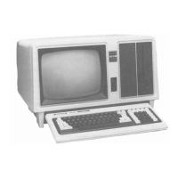
Tandy 1000
THEORY OF OPERATION
Main Logic Board
Technical Reference Manual
The
Block Diagram
of
the main logic board (Figure
3)
shows the basic functional
divisions.
CPU Function
The CPU function consists of the CPU (Intel 8088), the address, data inter-
face, the
CPU
control signal generator, the bus control signal generator and
the interrupt controller (Intel 8259A).
It
is
located
in
the upper right hand corner
of the board above the external bus connectors.
Non-CPU Function, Main Logic Board
The non-CPU functions can be divided into two main parts: memory and I/O.
Memory consists of
RAM
and ROM. RAM or Video/System Memory serves
as
storage for both the video data and program data.
ROM
memory contains
the
BIOS
and diagnostics. I/O consists of
all
the peripheral functions; keyboard,
floppy disk controller, printer, joystick, light pen and sound.
Processor Address/Data Interface
The 8088 has three groups of Address/Data lines;
ADO
- AD7, A8 - A15 and
A16 - A19.
ADO
- AD7 are multiplexed address and data lines.
To
separate
and save the address that comes out first, the signals are applied to
U61
(74LS373) and latched by ALE. Additionally, the signals are applied to data
transceiver U62 (74LS245). U62
is
enabled only during the data portion of
the
CPU
cycle.
(The
exception
is
during
an
Interrupt Acknowledge cycle.) Direc-
tion of transmission
is
controlled by the RD* (READ) signal from the CPU.
Address lines A8 - A15 are present during the entire CPU cycle and need only
to
be buffered. Address lines A16 - A19 are multiplexed with status signals
S4
-
S7
and need to be latched. The results
are:
A8
- A11, A16 -A19 are latched
into
U41
(74LS373) by ALE and A12 - A15 are buffered by half of U43
(74LS244). The outputs from these latches/buffers/transceivers are the BUS
Signals
AOO
- A19,
DO
- 07.
CPU Control Signal Generation
The 8088 CPU uses a 4.77 MHz clock with a special duty cycle (33% high,
67% low.) This clock
is
produced by the 8284 clock generator/driver U45. The
8284 receives a 14 MHz input clock and divides
it
by 3 to produce CPUCLK
(4.77 MHz) and by 6 to produce D2CLK (2.385 MHz).
In
addition to being
used by the control signal logic the clocks are buffered by U82 (74LS244) for
17
 Loading...