Tandy 1000
Technical Reference Manual
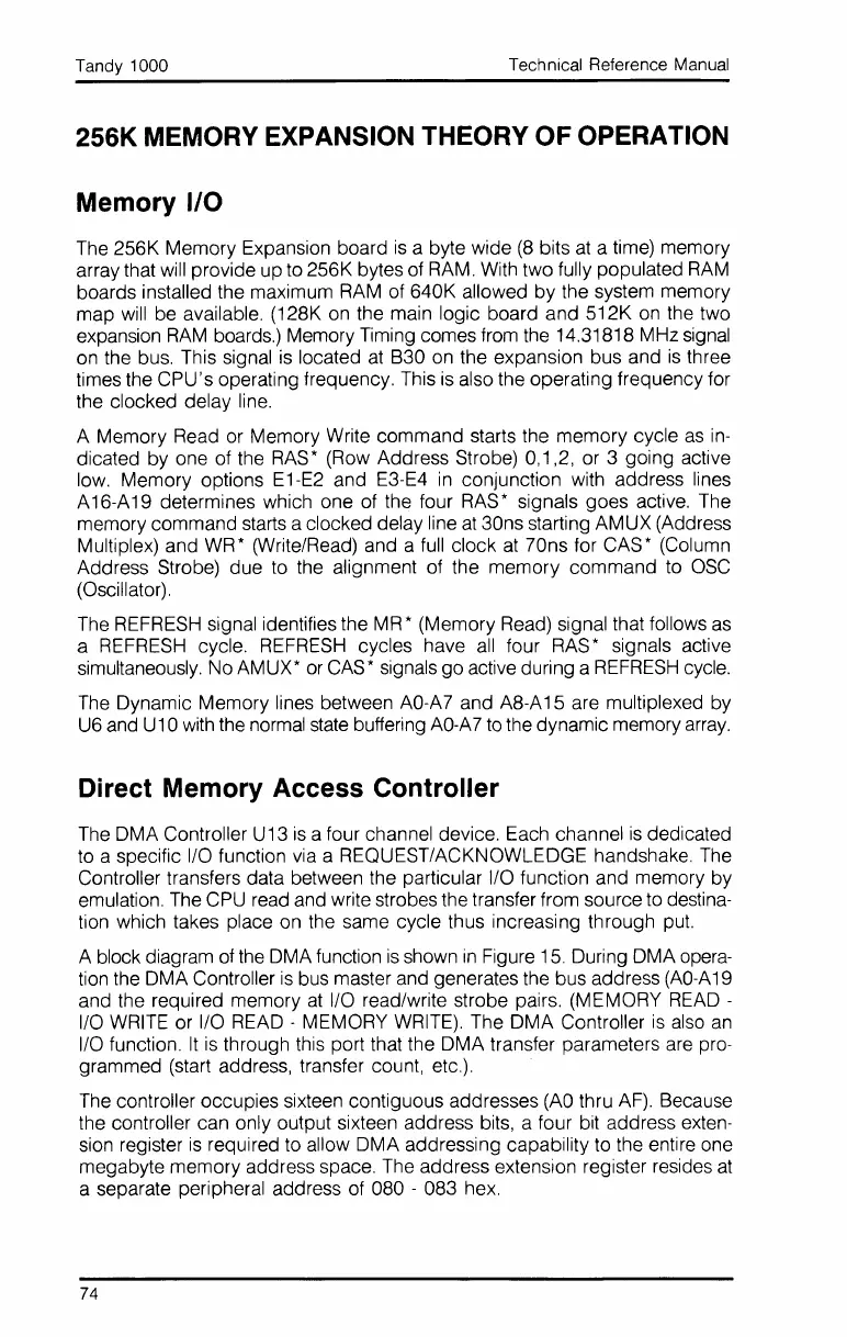
256K MEMORY EXPANSION THEORY
OF
OPERATION
Memory 1/0
The 256K Memory Expansion board
is
a byte wide
(8
bits
at
a time) memory
array that will provide up to 256K bytes of RAM. With two fully populated
RAM
boards installed the maximum RAM of 640K allowed by the system memory
map will be available. (128K on the main logic board and 512K
on
the two
expansion
RAM
boards.) Memory Timing comes from the 14.31818 MHz signal
on the bus. This signal
is
located
at
B30 on the expansion bus and
is
three
times the CPU's operating frequency. This
is
also the operating frequency for
the clocked delay line.
A Memory Read or Memory Write command starts the memory cycle
as
in-
dicated by one of the
RAS
* (Row Address Strobe) 0,1,2, or 3 going active
low. Memory options E1-E2 and E3-E4
in
conjunction with address lines
A16-A19 determines which one of the four
RAS
* signals goes active. The
memory command starts a clocked delay line
at
30ns starting AMUX (Address
Multiplex) and
WR
* (Write/Read) and a
full
clock
at
?Ons
for CAS *
(Col
umn
Address Strobe) due to the alignment of the memory command to
OSC
(Oscillator).
The REFRESH signal identifies the
MR
* (Memory Read) signal that follows
as
a REFRESH cycle. REFRESH cycles have
all
four
RAS
* signals active
simultaneously. No AMUX* or CAS* signals go active during a
REFRESH
cycle.
The Dynamic Memory lines between
AO-A?
and A8-A15 are multiplexed by
U6 and
U1
0 with the normal state buffering
AO-A?
to the dynamic memory array.
Direct Memory Access Controller
The DMA Controller U13
is
a four channel device. Each channel
is
dedicated
to a specific I/O function via a REQUEST/ACKNOWLEDGE handshake. The
Controller transfers data between the particular I/O function and memory by
emulation. The CPU read and write strobes the transfer from source to destina-
tion which takes place on the same cycle thus increasing through put.
A block diagram of the DMA function
is
shown
in
Figure 15. During DMA opera-
tion the DMA Controller
is
bus master and generates the bus address
(AO-A
19
and the required memory
at
I/O read/write strobe pairs. (MEMORY READ -
I/O WRITE or I/O READ - MEMORY WRITE). The
DMA
Controller
is
also
an
I/O function.
It
is
through this port that the DMA transfer parameters are pro-
grammed (start address, transfer count, etc.).
The controller occupies sixteen contiguous addresses
(AO
thru
AF).
Because
the controller can only output sixteen address bits, a four bit address exten-
sion register
is
required to allow DMA addressing capability to the entire one
megabyte memory address space. The address extension register resides
at
a separate peripheral address of 080 - 083 hex.
74
 Loading...