Tandy 1000
Technical Reference Manual
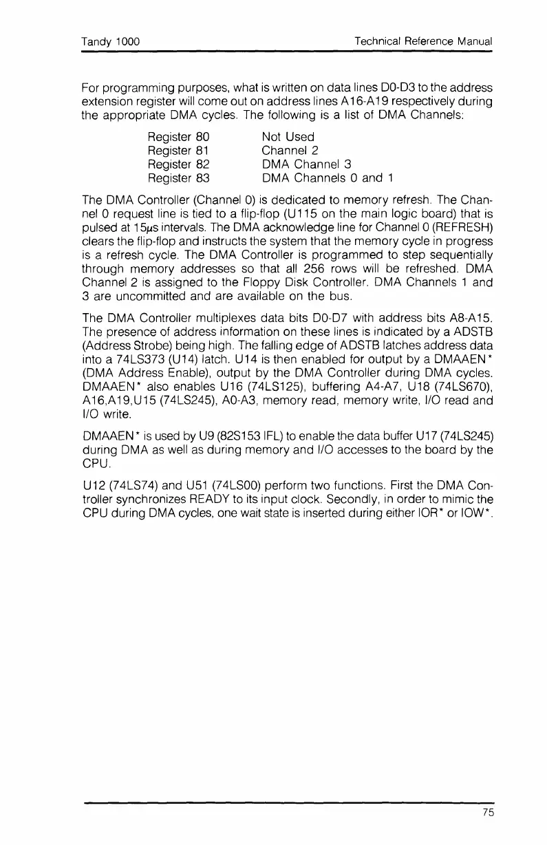
For programming purposes, what
is
written on data lines
00-03
to the address
extension register
will
come out on address lines A16-A19 respectively during
the appropriate OMA cycles. The following
is
a list of OMA Channels:
Register 80 Not Used
Register
81
Channel 2
Register 82 OMA Channel 3
Register 83 OMA Channels 0 and 1
The OMA Controller (Channel
0)
is
dedicated to memory refresh. The Chan-
nel 0 request line
is
tied to a flip-flop (U115 on the main logic board) that
is
pulsed
at
15Jis
intervals.
The
OMA acknowledge line for Channel 0
(REFRESH)
clears the flip-flop and instructs the system that the memory cycle
in
progress
is
a refresh cycle. The OMA Controller
is
programmed to step sequentially
through memory addresses so that
all
256 rows
will
be refreshed. OMA
Channel 2
is
assigned to the Floppy Disk Controller. OMA Channels 1 and
3 are uncommitted and are available on the bus.
The OMA Controller multiplexes data bits
00-07
with address bits A8-A
15.
The presence of address information on these lines
is
indicated by a AOSTB
(Address Strobe) being high. The falling
edge
of AOSTB latches address data
into a 74LS373
(U
14)
latch. U14
is
then enabled for output by a OMAAEN *
(OMA Address Enable), output by the OMA Controller during DMA cycles.
OMAAEN* also enables U16 (74LS125), buffering A4-A7, U18 (74LS670),
A16,A19,U15 (74LS245),
AO-A3,
memory read, memory write, I/O read and
I/O write.
OMAAEN *
is
used by
U9
(82S153
IFL)
to
enable the data buffer
U17
(74LS245)
during DMA
as
well
as
during memory and I/O accesses to the board by the
CPU.
U12 (74LS74) and
U51
(74LSOO)
perform two functions. First the DMA Con-
troller synchronizes READY
to
its input clock. Secondly,
in
order
to
mimic the
CPU during OMA cycles, one wait state
is
inserted during either IOR* or IOW*.
75
 Loading...