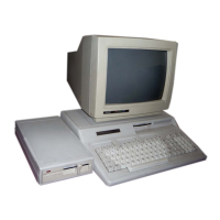
Tandy 1000
Floppy Disk Controller Interface
Technical Reference Manual
The Floppy Disk Controller interface consists of the 765 controller and sup-
port circuitry. The oscillator formed by U29,
Y1
generates an 8.00 MHz clock
that
is
divided down to 4.00 MHz and 2.00 MHz by U30. The 4.00 MHz signal
is
applied to the
FOC
for
its
internal processor clock
(ClK
pin 19) and to counter
circuit
U31
to generate the
FOC
write clock (WCK pin 21).
U31
produces a
pulse
at
count 15 that loads the next count of
8.
Therefore, WCK is a 250
nanosecond pulse every 2.0 microseconds. The CPU interface consists of the
chip select decode U98,
U51
address
AO,
A
1,
function decode FOCCS *, and
lOR
*, lOW
*.
The function decode
FOCOS
*
is
separated into the lower four
address range for the
"DaR"
register and into the upper four address range
for the
FOC;
both are inhibited by AEN. The
"DaR"
latch
U71
is
for configura-
tion control, drive select,
reset,
interruptiOMA request enable, drive motor con-
trol, and software transfer terminal count.
latch
U1
06
is
used to delay the
FOC
OMA request
(ORO)
as
specified by the 765 specification. Counter U50
is
used
to add pre-compensation
to
the MFM coded write data (250 nanosecond pulse
every 2.0 microseconds maximum). The 765 FOC signals
"early"
and
"late"
determine the number of 8 MHz clock periods (125 nanoseconds) the write
data
is
delayed thru U69 - normal =
6,
early =
4,
late =
7.
Data separator
U69 converts
"raw
data" from the drive into read data (ROD) and read clock
(ROW).
37
 Loading...