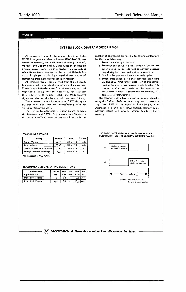
Tandy 1000
MC6845
Technical Reference Manual
SYSTEM BLOCK
DIAGRAM
DESCRIPTION
As
shown
in
Figure 1,
the
primary
function
of
the
CRTC
is
to
generate refresh addresses (MAO-MA13),
row
selects (RAO-RA41. and video
monitor
timing (HSYNC,
VSYNC) and Display Enable.
Other
functions
include an
internal
cursor
register which generates a
Cursor
output
when its
contents
compare
to
the
current
Refresh
Ad·
dress. A light-pen
strobe
input signal allows
capture
of
Refresh Address
in
an internal light pen register.
All timing
in
the
CRTC
is
derived from
the
Clk input.
In
alphanumeric
terminals, this signal
is
the
character
rate.
Character
rate
is
divided
down
from video
rate
by external
High
Speed
Timing
when
the
video
frequency
is
greater
than
3 MHz.
Shift
Register, Latch,
and
MUX
Control
signals are also provided by external High
Speed
Timing.
The processor
communicates
with
the
CRTC
through
a
buffered
8-bit
Data
BU5
by reading/writing
into
the
18-register file
of
the
CRTC.
The
Refresh
Memory
address
is
multiplexed
between
the
Processor
and
CRTC. Data appears
on
a
Secondary
Bus which
is
buffered
from
the
processor Primary Bus. A
MAXIMUM RATINGS
number
of
approaches
are
possible
for
solving
contentions
for
the
Refresh
Memory.
1. Processor always
gets
priority.
2.
Processor gets
priority
access
anytime,
but
can be
synchronized
by
an
interrupt
to
perform
accesses
only
during
horizontal
and
vertical retrace times.
3.
Synchronize
processor
by
memory
wait
cycles.
4.
Synchronize
processor
to
character
rate (See Figure
2). The
6800
MPU family lends itself
to
this config-
uration
because
it
has
constant
cycle lengths. This
method
provides
zero
burden
on
the
processor be-
cause
there
is
never a
contention
for
memory.
All
accesses are "transparent."
The secondary
data
bus
concept
in
no
way
precludes
using
the
Refresh RAM
for
other
purposes. It looks like
any
other
RAM
to
the
Processor.
For
example, using
Approach
4, a
64K
byte
RAM Refresh Memory
could
perform
refresh and program storage
functions
trans-
parently.
FIGURE
2 -
TRANSPARENT
REFRESH
MEMORY
CONFIGURATION
TIMING
USING
6800
MPU
FAMILY
Rating
Symbol
Supply
Voltage vee"
Input
Voltage
Vin"
Operating Temperature Range
TA
Storage
Temperature
Range
T
stg
·With
respect
to
VSS
(Gnd).
Value
Unit
-0.3
to
+7.0 Vdc
-0.3
to
+7.0 Vdc
o to +70
oc
-55
to
+150
oC
<1>1
I
CATC
Ace
••
,.,
I
Refresh
Memory
_
RECOMMENDED OPERATING
CONDITIONS
Characteristics
Supply
Voltage
Input
Low
Voltage
Input
High
Voltage
<1>2
I I
I I
~TCYCle;nXTcor~~:
I I
m,nare
integers;
T
c
is
character
period
®
MOTOROLA
Se,"iconductor
Product.
Inc.
 Loading...