Theory of Operation-PS
501
0
Keyboard
@
@
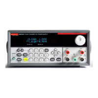
The front panel of this instrument has 20 momentary
contact SPST pushbutton switches shown on schematic 6.
These buttons are arranged in a 4 x 5 matrix. They are en-
coded by U1421 shown on schematic 4. This device is a
CMOS 20 key encoder. Scanning and debouncing circuitry
are included on this chip. Also included on
U1421 is an inter-
nal RAM that stores the last key pressed, even after the key
is released. The output of U1421 is tristate and is placed
directly on the data bus. When a key is pressed, pin 13 (data
available) goes high. This signals the microprocessor that a
keyboard entry has been made.
Output Control
@@
The CPU boapd outputs nine bits to the two analog
boards. Four of the nine bits are the two clock and two data
lines from U1411. The microprocessor programs the voltage
and current DACs in serial format through these four bits.
These lines go to shift registers on the analog boards.
The logic and floating supply output relays are controlled
via
U1411 pin 7 and U1315 pin 11, respectively, shown on
schematic 5.
The data strobe line that transfers the shift register bits
to the DACs is pin 10 of U1315 shown on schematic
5.
Pins
7
and
9
of U 131
5
have control over the floating supply mode
relays. These set the overhead voltage for either the high or
low output voltage mode.
Front-Panel Display
Gee
The front panel of this instrument has nine '/-segment
LEDs shown on schematic 6. The negative and positive sup-
ply LEDs (the first
6
counting from left to right) are
multiplexed by U1400, shown on schematic 5. This
multiplexer is a 6 digit BCD display controller and driver.
This device has six RAM locations. These are selected by
pins 26,
27,
and 28. These RAMS contain the information
that is written on the seven-segment LEDs. This device has
an internal oscillator that runs at approximately 300
Hz.
The
display refreshing is automatically accomplished without in-
tervention from the processor.
The first six common cathode seven-segment LEDs are
driven from U14OO through transistors Q1040, Q1132,
Q1131, Q1121, Q1120, and Q1122, shown on schematic
6.
Pin 1
6
of U 1 400 is used for duty cycle brightness control. By
varying the duty cycle of the waveform at pin 16, the dis-
plays are dimmed when the unit is in the program mode.
The duty cycle is controlled by
U1301 (shown on sche-
matic
5),
a data selector and U1315, an addressable latch.
When the microprocessor calls for a bright digit, it writes a
logic 1 at U1315. This gates a logic 0 through U1301 to the
display controller IC. If the microprocessor writes a logic 0
to U1315, the data selector gates a 20 kHz, 40% duty cycle
signal to the display controller IC causing the seven-seg-
ment LEDs to dim.
The remaining three seven-segment LEDs are
multiplexed by
U1410. This integrated circuit is similar to
U1400, except each LED segment is controlled indepen-
dently rather than with BCD data. This multiplexer scans at
a 500
Hz
rate and is capable of driving four seven-segment
LEDs. The LEDs that are equivalent electrically to the fourth
segment are the AMPS and VOLTS lights for the three sup-
plies, the ERROR and the NOT ENTERED lights. The three
AMPS and VOLTS LEDs are either on, off, or flashing. The
NOT ENTERED and ERROR LEDs are either off or flashing.
To achieve the flash capability, bus (62 is divided to 1.2 Hz
by U1322 and U1221. This 1.2
Hz
square wave is gated by
an addressable latch, U1314, and fed to U1412, an octal
buffer. To flash the LED, the M6800 writes a logic 1 into
U1410 and a logic 1 into U1314. IC U1314 acts as a switch
through AND gates
U1321, U13238, and Ul32l C. These
pass
the 1.2
Hz
square wave to the cathodes of the LEDs.
When the microprocessor writes a logic 0 into U1314, the
flashing stops and the LED is continuously on.
The remaining three LEDs (REMOTE, ADDRESSED, and
OUTPUT ON) are controlled by addressable latch Ul4ll
shown on schematic 4. The REMOTE and ADDRESSED
LEDs are illuminated with logic 0 into U1411. The OUTPUT
LCD
is
illuminated with
a
logic
1.
Ground Referenced Circuits
0
The +26 V from the mainframe is applied at interface
pins 12A and
B.
This voltage passes through F1340 to the
collector of Q1440. The base of Q1440 is set at about
+
16 V by VR1341.
+
15 V is available at the emitter of
Q144O. The
-
26 V from the mainframe passes through
F1341 to the collector of Ql44l. The base of Q1441 is set
by VRl34O at about
-
16 V.
-
15 V is available at the
emitter of (31441.
+
8 V from the mainframe passes through
F1250, and is filtered by L1240. C1120 and C1231. A
crowbar circuit is formed by Q1240. An RC time constant at
the gate of Q1240 is formed by R1130 to C1230 and
R1132. Drive for the crowbar is provided by Q1130 and
Q123O. If either the
+
5
V at the emitter of Q123O or logic
supply sense at the emitter of Q1130 goes more than
-700 mV positive than the base voltage, the respective
transistor turns on. This action fires Q1240, which opens
the input fuse or trips the mainframe current limit.
Five relays and drivers are shown on this schematic.
They are the floating supply output relay, floating supply
sense relay, logic supply output relay,
+
mode relay and
-
REV
SEP 1981
 Loading...