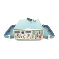
Theory
of
Operation-PS
501
0
Fold-back current limit is provided by U1540. IC U1540
functions similar to current error amplifier U1640, except the
reference voltage is related to the supply output voltage.
This reference is produced by divider network R1541,
R1542, and R1543. With an output voltage of 4
V,
the cur-
rent limit is about
3
A. At 0 V, output current limit is less
than 1 A.
Floating Supply Rectifiers and Filters
Each of the floating supplies in the PS 5010 has two in-
ternal operating modes. These are the high voltage and low
voltage modes. Output voltages from 0 V to 32 V are avail-
able In the high voltage mode, and 0 V to 15 V in the low
voltage mode. The operating mode is determined by the
programmed current limit. Low voltage mode above 400
mA
In a standard mainframe compartment occurs with current
limits. and above 750 mA in a high power compartment.
The
+
and
-
floating supply voltages come from four
isolated 25
V
ac windings located in the power module. As
shown on the schematic, only the center two windings sup-
ply current in the low voltage modes. The maximum current
available from these supplies depends on whether the plug-
in is in a high power or standard compartment.
The return for the
+
supply is ground 3, and the return
for the
-
supply is ground 4. These grounds are connected
through current sensing resistors R1104 and R1105 to form
the output common (ground 1). Grounds 3 and 4 are used
throughout the circu~try to avo~d generating errors in the
current limit. Current drawn from any positive voltage and
returned through ground 3 doesn't affect either current limit.
Current drawn from ground 4 and returned through any neg-
ative voltage will not affect either current limit; however, any
current drawn from the
+
output must return through the
+
sense resistor. The same occurs in the negative supply.
The ac from the power module is fused and passes to
four bridge rectifiers. C1710, C1620, C1711, and C1910 re-
duce commutation noise entering the dc bus. The two di-
odes shown before the bridge rectifiers supply additional
voltage for the base drive regulators as described later.
After passing through the bridge rectifiers, the pulsating di-
rect current is filtered by a choke input filter. Chokes L500A
and LSOOB, as well as L510A and L5106, are mutually
coupled.
The collector voltage for the series pass-transistors in
the mainframe is relay switched depending on the output
voltage mode selected. Relays
K1510 and K2010 switch the
collector and base drive voltages for the series pass-transis-
tors. The supplies are stacked to obtain the higher dc
voltages.
Base drwe for the
+
supply series pass-transistor is pro-
v~ded by emitter followers Q1500 in the high voltage mode
and Q1501 ~n the low voltage mode. Transistors (22000 and
Q1900 perform the same function for the
-
supply. Correct
base voltages for these transistors are provided by Zener
diodes
VR1501 and VR1600 and in the
-
supply, VR2000
and VR1800. Constant current for these Zeners is provided
by (21600 and VR1500 (Q1901 and VR1900 in the
-
supply).
A
constant current load for the
+
collector supply is pro-
vided by current source Q1800, R1811, and VR1701
(Ql700, R1711, and VRl7OO in the
-
supply).
A
constant
current of about 25
mA
flows from Q1800 to the
-
supply
output. Likewise, 25 mA flows from the
+
supply output,
through Q1700, into the
-
collector supply. The positive
current source is connected to the anode of CR1800. The
negative current source is connected to the cathode of
CR1700. When the supplies power down, the regulator
ceases operation before the filter capacitors fully discharge.
CR1800 becomes a positive current source and CR1700 a
negative current sink. These diodes provide an alternate dis-
charge path for capacitance in the opposite polarity supply
during shutdown.
Floating Supply Digital-to-Analog Converter
circuits
@
The data, clock, and transfer strobe are applied to opto-
isolators U1030, U1041, and U1042. These isolators are
necessary, as the CPU circuitry is referenced to chassis
ground and the floating supply circuitry is not. The output of
the optoisolators drives the emitters of level shifting transis-
tors Q1140, Q1141, and (21142.
The
base current for these
transistors is provided by (21143 with associated compo-
nents. The output voltage of this emitter follower is 2 V.
These level shift transistors permit higher speed operation
for the transistors in the optoisolators, as only a small volt-
age change is required at the collectors of the optoisolator
transistors.
The registers
U1140, U1240, Ul241, U1121 and
U1242
are shift-and-store devices similar to the ones used in the
logic supply. The serial data input is accumulated in time
with the clock pulse inputs. When the transfer strobe pulse
occurs, the registered data transfers to the device's internal
latches. A total of 37 output bits are used. Bits 33 through
36 pass to the
FET
gain switches shown on schematics 11
and 12. Bit 37 disables the voltage reference. The remaining
bits go directly to the digital-to-analog converters.
Four DACs are used in this circuit. The
-
current refer-
ence is generated by
U
1221 and U 1 1 1 1 A. The
+
current
reference is generated by U1230 and U1111 B. The
+
volt-
age reference is generated by U1130 and U 1330B, while the
-
voltage reference is generated by U1231 and U1330A.