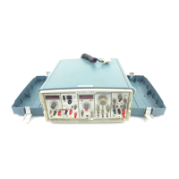
Theory of Operation-PS 50
10
System Clock
@
1
The M6800 is driven by a two-phase, nonoverlapping
clock signal. The clock is generated by a three transistor
(Q1120, Q1121, Q1122) RC oscillator that includes R1223,
R1220, R1128, and C1122. The oscillator runs at 4 MHz.
This signal is divided to 1 MHz
by
two
flip-flops, U1220A
and U1220B. Bus 42 (1 MHz clock) is taken directly from pin
9
of U1220B. Clock signals (1 MHz) MPU
$1
and MPU 42
are supplied from pins 13 and 10 of U1112D and U1112C,
respectively. NOR gate U1112C and U1112D insures that
MPU
(/,I
and MPU
42
are nonoverlapping.
Chip
Selects
@
Chip selects for the following are generated by U1120.
VMA and 42 are included in the chip enable for U1120.
Table 4-1
U
1 120 CHlP SELECTS
Chip
Selects
@
Ch~p selects for the following are generated by U1310.
Address
0000-1 FFF
COOO-DFFF
E000-FFFF
8000-9FFF
A000-BFFF
Circuit Number
U1300, U1302
U1200, U1201
ROM
ROM
ROM
ROM
Latch
Latch
Type
RAM
ROM
Table
4-2
U
13
10
CHlP SELECTS
COOO-CFFF
D000-DFFF
E000-EFFF
FOOO-FFFF
3000-303F
3040-307 F
U1100, U1101 ROM
U1001 GPIB
U1212 Switch
Address
Circuit Number
VMA is used only in Ul411, U1314, and U1315.
Type
U1315
The remaining chip selects are produced by U13ll and
are:
Table 4-3
U
13
1
1
CHlP SELECTS
Latch
Circuit Number
3080-30BF
VMA is included in
Memory
@
Keyboard 2800-2BFF
Display 2400-27FF
Display 2000-23FF
all Ul3ll chip selects.
Located
the CPU board are 16k bytes of ROM con-
taining the operating system firmware. This instrument has
either
2
8kx8 or 4 4kx8 ROMs. Table 4-4 shows the location
and addresses of these ROMs.
Table 4-4
OPERATING SYSTEM FIRMWARE
LOCATIONS AND ADDRESSES
There are seven input lines from the analog boards.
These pass information to the microprocessor via U1420,
an
8
bit, tristate buffer.
Six of the seven inputs lines are status bits from the
three supplies. These consist of two lines for each supply, a
current and voltage regulation line. The status bits tell the
microprocessor whether the supplies are in voltage or cur-
rent regulation or unregulated. The seventh bit is a high
power indicator. This informs the microprocessor that the
PS 5010 is in the high power compartment
of
the power
module.
Address
System RAM
@
System RAM consists of U 1300 and U 1302. These pro-
vide temporary operating memory. These RAMS are
1024
x
4 bit arranged in a 1024 x 8 bit pattern at address
0000-03FF. These are fully static devices.
Circuit
Number
Circuit
Number
Address