AM3359, AM3358, AM3357, AM3356, AM3354, AM3352
www.ti.com
SPRS717H –OCTOBER 2011–REVISED MAY 2015
7.7.2.3.3.8 Net Classes
Table 7-64 lists the clock net classes for the DDR3 interface. Table 7-65 lists the signal net classes, and
associated clock net classes, for signals in the DDR3 interface. These net classes are used for the
termination and routing rules that follow.
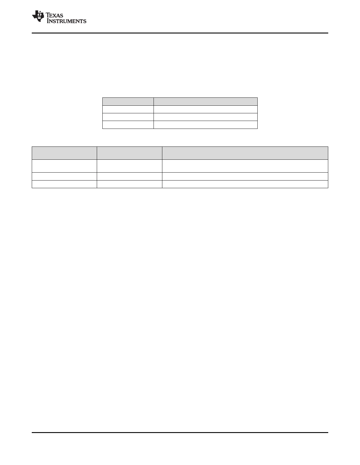
Table 7-64. Clock Net Class Definitions
CLOCK NET CLASS AM335x PIN NAMES
CK DDR_CK and DDR_CKn
DQS0 DDR_DQS0 and DDR_DQSn0
DQS1 DDR_DQS1 and DDR_DQSn1
Table 7-65. Signal Net Class Definitions
ASSOCIATED CLOCK NET
SIGNAL NET CLASS AM335x PIN NAMES
CLASS
DDR_BA[2:0], DDR_A[15:0], DDR_CSn0, DDR_CASn, DDR_RASn,
ADDR_CTRL CK
DDR_WEn, DDR_CKE, DDR_ODT
DQ0 DQS0 DDR_D[7:0], DDR_DQM0
DQ1 DQS1 DDR_D[15:8], DDR_DQM1
7.7.2.3.3.9 DDR3 Signal Termination
Signal terminations are required for the CK and ADDR_CTRL net class signals. On-device terminations
(ODTs) are required on the DQS[x] and DQ[x] net class signals. Detailed termination specifications are
covered in the routing rules in the following sections.
Figure 7-48 provides an example DDR3 schematic with a single 16-bit DDR3 memory device that does
not have V
TT
termination on the address and control signals. A typical DDR3 point-to-point topology may
provide acceptable signal integrity without V
TT
termination. System performance should be verified by
performing signal integrity analysis using specific PCB design details before implementing this topology.
7.7.2.3.3.10 DDR_VREF Routing
DDR_VREF is used as a reference by the input buffers of the DDR3 memories as well as the AM335x
device. DDR_VREF is intended to be half the DDR3 power supply voltage and is typically generated with
a voltage divider connected to the VDDS_DDR power supply. It should be routed as a nominal 20-mil wide
trace with 0.1 µF bypass capacitors near each device connection. Narrowing of DDR_VREF is allowed to
accommodate routing congestion.
7.7.2.3.3.11 VTT
Like DDR_VREF, the nominal value of the VTT supply is half the DDR3 supply voltage. Unlike
DDR_VREF, VTT is expected to source and sink current, specifically the termination current for the
ADDR_CTRL net class Thevinen terminators. VTT is needed at the end of the address bus and it should
be routed as a power sub-plane. VTT should be bypassed near the terminator resistors.
7.7.2.3.4 DDR3 CK and ADDR_CTRL Topologies and Routing Definition
The CK and ADDR_CTRL net classes are routed similarly and are length matched to minimize skew
between them. CK is a bit more complicated because it runs at a higher transition rate and is differential.
The following subsections show the topology and routing for various DDR3 configurations for CK and
ADDR_CTRL. The figures in the following subsections define the terms for the routing specification
detailed in Table 7-66.
Copyright © 2011–2015, Texas Instruments Incorporated Peripheral Information and Timings 181
Submit Documentation Feedback
Product Folder Links: AM3359 AM3358 AM3357 AM3356 AM3354 AM3352
 Loading...