A1 A2
AM335x
Address and Control
Output Buffer
DDR3 Address and Control Input Buffers
AT
Vtt
Address and Control
Terminator
Rtt
AS
A1 A2
AM335x
Differential Clock
Output Buffer
DDR3 Differential CK Input Buffer
Routed as Differential Pair
AT
Rcp
Clock Parallel
Terminator
A1 A2
AT
AS-
AS+
Rcp
Cac
VDDS_DDR
0.1 µF
+
–
+
–
AM3359, AM3358, AM3357, AM3356, AM3354, AM3352
www.ti.com
SPRS717H –OCTOBER 2011–REVISED MAY 2015
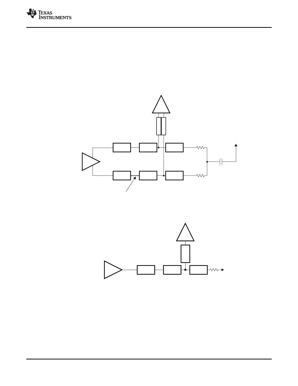
7.7.2.3.4.2 One DDR3 Device
A single DDR3 device is supported on the DDR3 interface consisting of one x16 DDR3 device arranged
as one 16-bit bank.
7.7.2.3.4.2.1 CK and ADDR_CTRL Topologies, One DDR3 Device
Figure 7-58 shows the topology of the CK net classes and Figure 7-59 shows the topology for the
corresponding ADDR_CTRL net classes.
Figure 7-58. CK Topology for One DDR3 Device
Figure 7-59. ADDR_CTRL Topology for One DDR3 Device
Copyright © 2011–2015, Texas Instruments Incorporated Peripheral Information and Timings 185
Submit Documentation Feedback
Product Folder Links: AM3359 AM3358 AM3357 AM3356 AM3354 AM3352
 Loading...