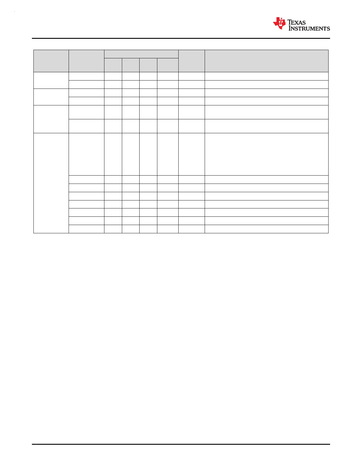
Table 6-3. Signal Descriptions (continued)
FUNCTION
SIGNAL
NAME
PIN NO.
(1)
PIN TYPE
(2)
DESCRIPTION
64 PM
48 PT,
RGZ
32
RHB
28
DGS28
BSL (I
2
C)
BSLSCL 34 2 2 5 I/O Default I
2
C BSL clock
BSLSDA 33 1 1 4 I/O Default I
2
C BSL data
BSL (UART)
BSLRX 57 19 15 16 I Default UART BSL receive
BSLTX 56 18 14 15 O Default UART BSL transmit
CAN
CAN_TX
5
30
27
46
16
30
1 O CAN-FD transmit data
CAN_RX
6
31
28
47
17
31
2 I CAN-FD receive data
Clock
CLK_OUT
7
18
39
49
55
56
63
5
13
17
18
29
40
11
13
14
18
26
14
15
17
25
O Configurable clock output
HFCLK_IN 46 12 10 13 I Digital high-frequency clock input
HFXIN 45 11 9 12 I Input for high-frequency crystal oscillator HFXT
HFXOUT 46 12 10 13 O Output for high-frequency crystal oscillator HFXT
LFCLK_IN 44 10 8 11 I Digital low-frequency clock input
LFXIN 43 9 7 10 I Input for low-frequency crystal oscillator LFXT
LFXOUT 44 10 8 11 O Output of low-frequency crystal oscillator LFXT
ROSC 42 8 6 9 I External resistor used for improving oscillator accuracy
MSPM0G3507, MSPM0G3506, MSPM0G3505
SLASEX6A – FEBRUARY 2023 – REVISED JUNE 2023
www.ti.com
16 Submit Document Feedback
Copyright © 2023 Texas Instruments Incorporated
Product Folder Links: MSPM0G3507 MSPM0G3506 MSPM0G3505
 Loading...


