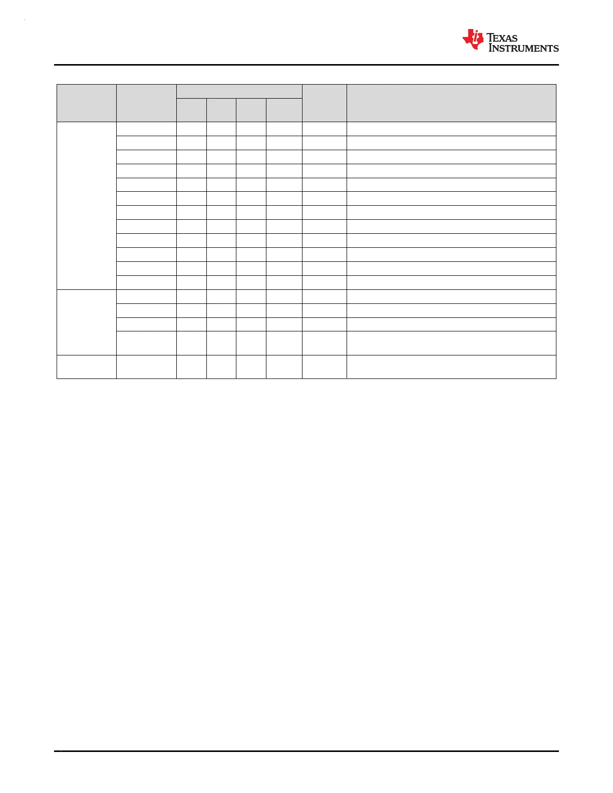
Table 6-3. Signal Descriptions (continued)
FUNCTION
SIGNAL
NAME
PIN NO.
(1)
PIN TYPE
(2)
DESCRIPTION
64 PM
48 PT,
RGZ
32
RHB
28
DGS28
Operational
Amplifier with
Chopping
(Zero-Drift Op-
Amp)
OPA0_IN0+ 30 46 30 1 I OPA0 non-inverting terminal input 0
OPA0_IN1+ 26 45 29 28 I OPA0 non-inverting terminal input 1
OPA0_IN2+ 8 30 19 18 I OPA0 non-inverting terminal input 2
OPA0_IN0- 31 47 31 2 I OPA0 inverting terminal input 0
OPA0_IN1- 25 44 28 27 I OPA0 inverting terminal input 1
OPA0_OUT 18 40 26 25 O OPA0 output
OPA1_IN0+ 16 38 – – I OPA1 non-inverting terminal input 0
OPA1_IN1+ 11 33 22 21 I OPA1 non-inverting terminal input 1
OPA1_IN2+ 8 30 19 18 I OPA1 non-inverting terminal input 2
OPA1_IN0- 19 41 – – I OPA1 inverting terminal input 0
OPA1_IN1- 10 32 21 20 I OPA1 inverting terminal input 1
OPA1_OUT 9 31 20 19 O OPA1 output
Power
VSS 41 7 5 8 P Ground supply
VDD 40 6 4 7 P Power supply
VCORE 32 48 32 3 P Regulated core power supply output
QFN Pad – Pad Pad – P
QFN package exposed thermal pad. TI recommends
connection to V
SS
.
RTC RTC_OUT
31
55
17
47
13
31
2
14
O RTC clock output
MSPM0G3507, MSPM0G3506, MSPM0G3505
SLASEX6A – FEBRUARY 2023 – REVISED JUNE 2023
www.ti.com
20 Submit Document Feedback
Copyright © 2023 Texas Instruments Incorporated
Product Folder Links: MSPM0G3507 MSPM0G3506 MSPM0G3505
 Loading...


