7.20.1 SPI (continued)
over operating free-air temperature range (unless otherwise noted)
PARAMETERS TEST CONDITIONS MIN TYP MAX UNIT
t
HD.CO
PICO output data hold time
(3)
1 ns
Peripheral
t
CS.LEAD
CS lead-time, CS active to clock 8 ns
t
CS.LAG
CS lag time, Last clock to CS
inactive
1 ns
t
CS.ACC
CS access time, CS active to POCI
data out
23 ns
t
CS.DIS
CS disable time, CS inactive to
POCI high inpedance
19 ns
t
SU.PI
PICO input data setup time 7 ns
t
HD.PI
PICO input data hold time 31.25 ns
t
VALID.PO
POCI output data valid time
(2)
2.7 < VDD < 3.6V 24 ns
t
VALID.PO
POCI output data valid time
(2)
1.62 < VDD < 2.7V 31 ns
t
HD.PO
POCI output data hold time
(3)
12 ns
(1) The POCI input data setup time can be fully compensated when delayed sampling feature is enabled.
(2) Specifies the time to drive the next valid data to the output after the output changing SCLK clock edge
(3) Specifies how long data on the output is valid after the output changing SCLK clock edge
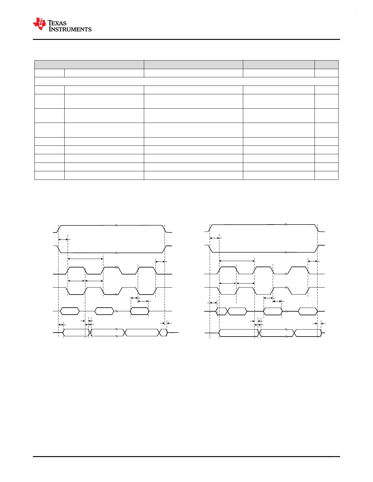
7.20.2 SPI Timing Diagram
SCLK
(SPO = 0)
POCI
SCLK
(SPO = 1)
CS
(inverted)
CS
PICO
t
CS, LEAD
t
CS, ACC
t
CS, LAG
t
CS, DIS
t
SU,CI
t
HD,CI
t
VALID,CO
t
HD,CO
1 / f
SPI
t
SCLK_H/L
t
SCLK_H/L
Controller Mode, SPH = 0
CS
(inverted)
CS
t
CS, LEAD
t
CS, ACC
t
CS, LAG
t
CS, DIS
t
SU,CI
t
HD,CI
t
VALID,CO
t
HD,CO
SCLK
(SPO = 0)
POCI
SCLK
(SPO = 1)
PICO
1 / f
SPI
t
SCLK_H/L
t
SCLK_H/L
Controller Mode, SPH = 1
Figure 7-6. SPI timing diagram - Controller Mode
www.ti.com
MSPM0G3507, MSPM0G3506, MSPM0G3505
SLASEX6A – FEBRUARY 2023 – REVISED JUNE 2023
Copyright © 2023 Texas Instruments Incorporated
Submit Document Feedback
49
Product Folder Links: MSPM0G3507 MSPM0G3506 MSPM0G3505