Table 8-4. Memory Organization (continued)
MEMORY REGION SUBREGION MSPM0G3505 MSPM0G3506 MSPM0G3507
Subsystem
0x6000.0000 to
0x7FFF.FFFF
0x6000.0000 to
0x7FFF.FFFF
0x6000.0000 to
0x7FFF.FFFF
System PPB
0xE000.0000 to
0xE00F.FFFF
0xE000.0000 to
0xE00F.FFFF
0xE000.0000 to
0xE00F.FFFF
(1) First 32KB flash memory (address 0x0000.0000 to 0x0000.8000) has up to 100000 program/erase cycles.
(2) If the DMA controller is to be configured for DMA transfers which access the SRAM, the ECC protected SRAM address region must
not be used by the DMA or the CPU. In cases where the DMA must access SRAM, configure the DMA and CPU to use only the parity
checked SRAM address region or the unchecked SRAM address region
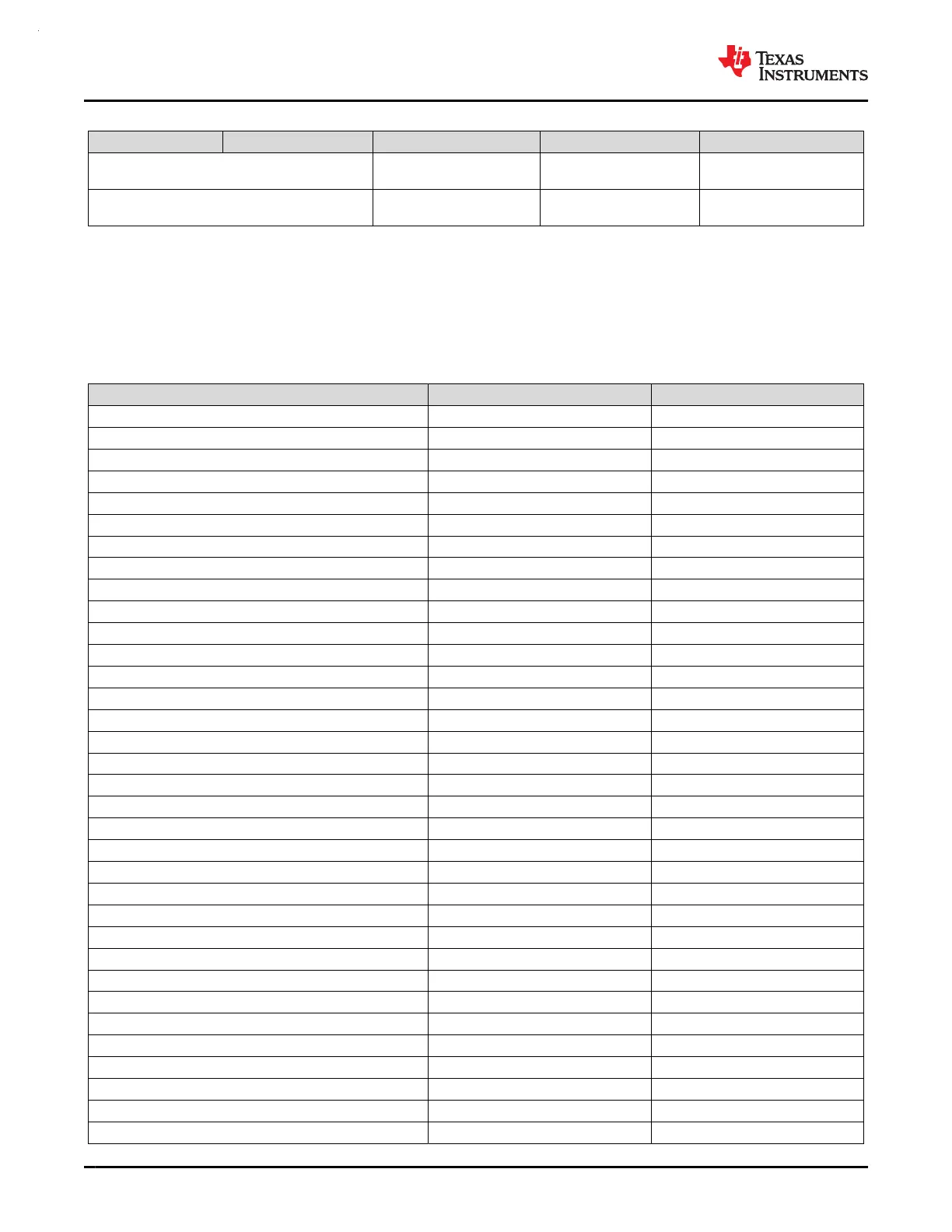
8.7.2 Peripheral File Map
Table 8-5 lists the available peripherals and the register base address for each.
Table 8-5. Peripherals Summary
Peripheral Name Base Address Size
COMP0 0x40008000 0x2000
COMP1 0x4000A000 0x2000
COMP2 0x4000C000 0x2000
DAC_OUT 0x40018000 0x2000
OPA0 0x40020000 0x2000
OPA1 0x40022000 0x2000
VREF 0x40030000 0x2000
WWDT0 0x40080000 0x2000
WWDT1 0x40082000 0x2000
TIMG0 0x40084000 0x2000
TIMG8 0x40090000 0x2000
RTC 0x40094000 0x2000
GPIO0 0x400A0000 0x2000
GPIO1 0x400A2000 0x2000
SYSCTL 0x400AF000 0x3000
DEBUGSS 0x400C7000 0x2000
EVENT 0x400C9000 0x3000
NVMNW 0x400CD000 0x2000
I2C0 0x400F0000 0x2000
I2C1 0x400F2000 0x2000
UART1 0x40100000 0x2000
UART2 0x40102000 0x2000
UART0 0x40108000 0x2000
MCPUSS 0x40400000 0x2000
MATHACL 0x40410000 0x2000
WUC 0x40424000 0x1000
IOMUX 0x40428000 0x2000
DMA 0x4042A000 0x2000
CRC 0x40440000 0x2000
AES 0x40442000 0x2000
TRNG 0x40444000 0x2000
SPI0 0x40468000 0x2000
SPI1 0x4046A000 0x2000
UART3 0x40500000 0x2000
MSPM0G3507, MSPM0G3506, MSPM0G3505
SLASEX6A – FEBRUARY 2023 – REVISED JUNE 2023
www.ti.com
58 Submit Document Feedback
Copyright © 2023 Texas Instruments Incorporated
Product Folder Links: MSPM0G3507 MSPM0G3506 MSPM0G3505
 Loading...


