RM46L852
SPNS185 –SEPTEMBER 2012
www.ti.com
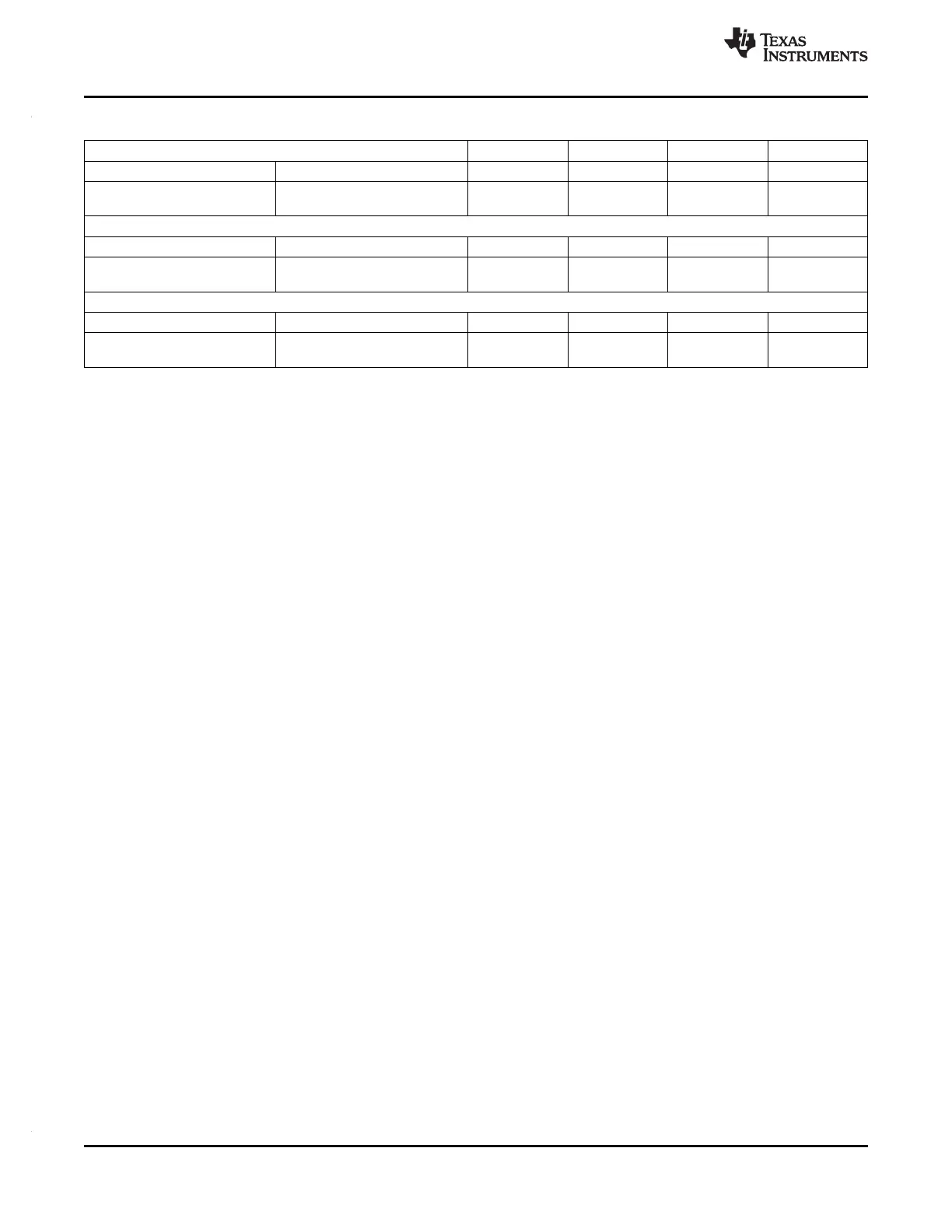
Table 5-21. MibADC Timing Specifications
Parameter MIN NOM MAX Unit
t
c(ADCLK)
(1)
Cycle time, MibADC clock 0.033 µs
t
d(SH)
(2)
Delay time, sample and hold 0.2 µs
time
12-bit mode
t
d©)
Delay time, conversion time 0.4 µs
t
d(SHC)
(3)
Delay time, total sample/hold 0.6 µs
and conversion time
10-bit mode
t
d©)
Delay time, conversion time 0.33 µs
t
d(SHC)
(3)
Delay time, total sample/hold 0.53 µs
and conversion time
(1) The MibADC clock is the ADCLK, generated by dividing down the VCLK by a prescale factor defined by the ADCLOCKCR register bits
4:0.
(2) The sample and hold time for the ADC conversions is defined by the ADCLK frequency and the AD<GP>SAMP register for each
conversion group. The sample time needs to be determined by accounting for the external impedance connected to the input channel as
well as the ADC’s internal impedance.
(3) This is the minimum sample/hold and conversion time that can be achieved. These parameters are dependent on many factors, e.g the
prescale settings.
132 Peripheral Information and Electrical Specifications Copyright © 2012, Texas Instruments Incorporated
Submit Documentation Feedback