V
S1
On-State
Leakage
Off-State
Leakages
V
S2
V
S24
39*I
AIL
I
AIL
I
AIL
R
ext
R
ext
R
ext
P
in
S
mux
R
mux
P
in
S
mux
R
mux
P
in
S
mux
R
mux
S
samp
R
samp
C
samp
C
ext
I
AIL
I
AIL
I
AIL
I
AIL
C
mux
C
ext
C
ext
RM46L852
www.ti.com
SPNS185 –SEPTEMBER 2012
5.4.3 ADC Electrical and Timing Specifications
Table 5-19. MibADC Recommended Operating Conditions
Parameter MIN MAX Unit
AD
REFHI
A-to-D high-voltage reference source AD
REFLO
V
CCAD
V
AD
REFLO
A-to-D low-voltage reference source V
SSAD
AD
REFHI
V
V
AI
Analog input voltage AD
REFLO
AD
REFHI
V
I
AIC
Analog input clamp current - 2 2 mA
(VAI < VSSAD – 0.3 or VAI > VCCAD + 0.3)
Table 5-20. MibADC Electrical Characteristics Over Full Ranges of Recommended Operating Conditions
Parameter Description/Conditions MIN MAX Unit
R
mux
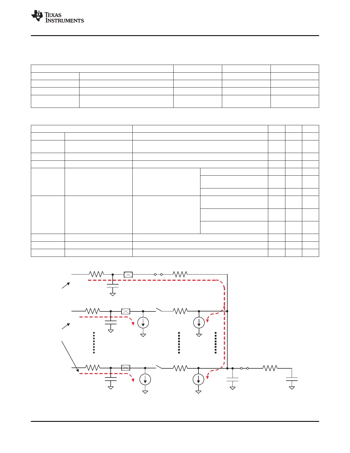
Analog input mux on-resistance See Figure 5-6 250 Ω
R
samp
ADC sample switch on- See Figure 5-6 250 Ω
resistance
C
mux
Input mux capacitance See Figure 5-6 16 pF
C
samp
ADC sample capacitance See Figure 5-6 13 pF
I
AIL
Analog off-state input leakage Off-state input leakage per V
SSAD
< V
IN
< V
SSAD
+ 100mV 300 nA
current, for V
CCAD
= 3.6V ADC input pin
V
SSAD
+ 100mV < V
IN
< V
CCAD
200 nA
maximum
- 200mV
V
CCAD
- 200mV < V
IN
< V
CCAD
500 nA
I
AIL
Analog off-state input leakage Off-state input leakage per V
IN
> V
SSAD
, 1 µA
current, for V
CCAD
= 5.5V ADC input pin V
IN
< V
SSAD
+ 300mV
maximum
V
IN
> V
SSAD
+ 300mV, 250 nA
V
IN
< V
CCAD
- 300mV
V
IN
> V
CCAD
- 300mV, 1 µA
V
IN
< V
CCAD
I
ADREFHI
AD
REFHI
input current AD
REFHI
= V
CCAD
, AD
REFLO
= V
SSAD
3 mA
I
CCAD
Static supply current Normal operating mode 15 mA
ADC core in power down mode 5 µA
Figure 5-6. MibADC Input Equivalent Circuit
Copyright © 2012, Texas Instruments Incorporated Peripheral Information and Electrical Specifications 131
Submit Documentation Feedback