RM46L852
SPNS185 –SEPTEMBER 2012
www.ti.com
4.6.3 Clock Test Mode
The platform architecture defines a special mode that allows various clock signals to be brought out on to
the ECLK pin and N2HET1[12] device outputs. This mode is called the Clock Test mode. It is very useful
for debugging purposes and can be configured via the CLKTEST register in the system module.
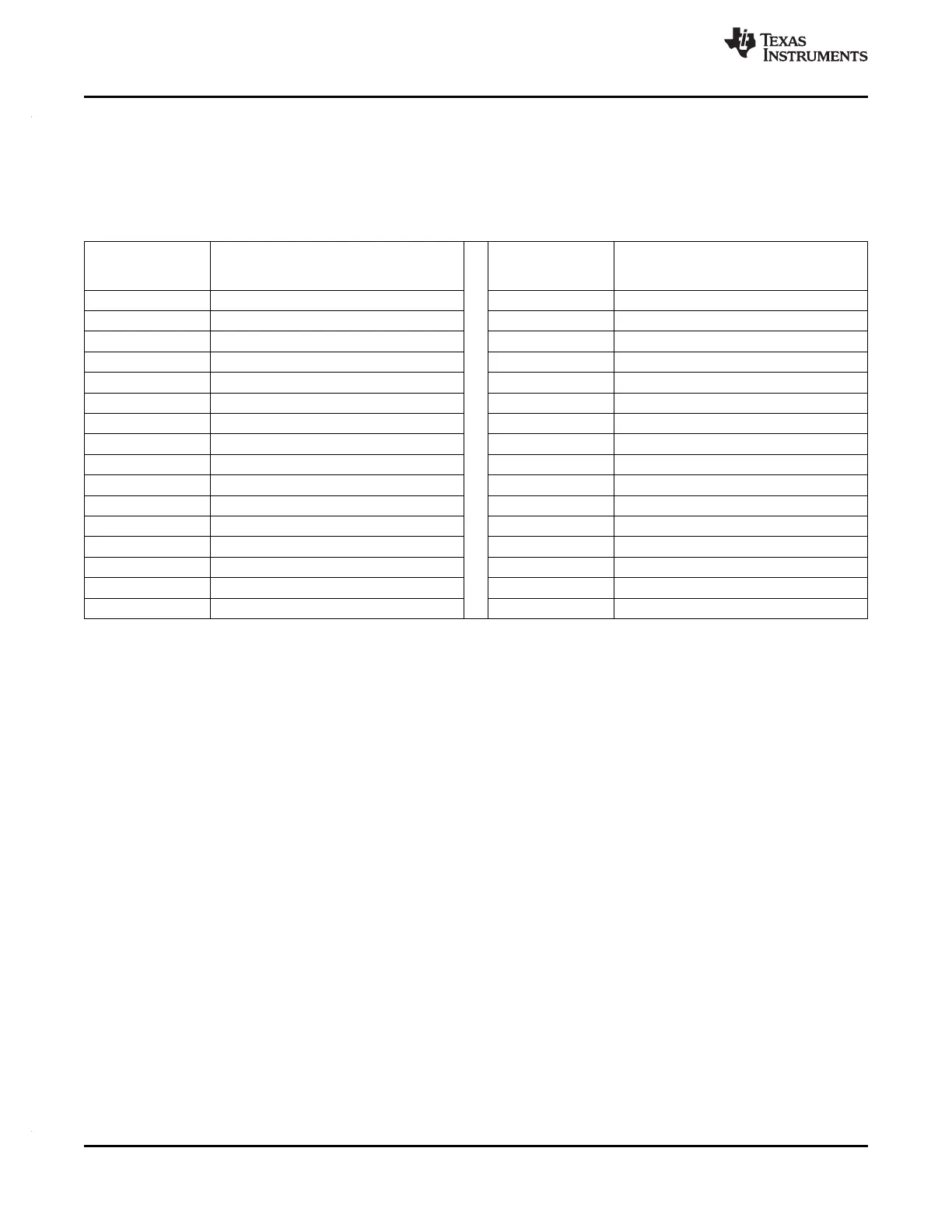
Table 4-15. Clock Test Mode Options
SEL_ECP_PIN SEL_GIO_PIN
= SIGNAL ON ECLK = SIGNAL ON N2HET1[12]
CLKTEST[3-0] CLKTEST[11-8]
0000 Oscillator 0000 Oscillator Valid Status
0001 Main PLL free-running clock output 0001 Main PLL Valid status
0010 Reserved 0010 Reserved
0011 EXTCLKIN1 0011 Reserved
0100 LFLPO 0100 Reserved
0101 HFLPO 0101 HFLPO Valid status
0110 Secondary PLL free-running clock output 0110 Secondary PLL Valid Status
0111 EXTCLKIN2 0111 Reserved
1000 GCLK 1000 LFLPO
1001 RTI Base 1001 Oscillator Valid status
1010 Reserved 1010 Oscillator Valid status
1011 VCLKA1 1011 Oscillator Valid status
1100 Reserved 1100 Oscillator Valid status
1101 VCLKA3_DIVR 1101 VCLKA3_S
1110 VCLKA4_DIVR 1110 VCLKA4_S
1111 Reserved 1111 Oscillator Valid status
70 System Information and Electrical Specifications Copyright © 2012, Texas Instruments Incorporated
Submit Documentation Feedback