VCLKA4_SRC
0
1
3
4
5
6
7
VCLK
VCLKA4_S(leftopen)
/DIVR
PLL2post_ODCLK/8
PLL2post_ODCLK/16
VCLKA4_DIVR_EMAC
(toEMAC)
RM46L852
www.ti.com
SPNS185 –SEPTEMBER 2012
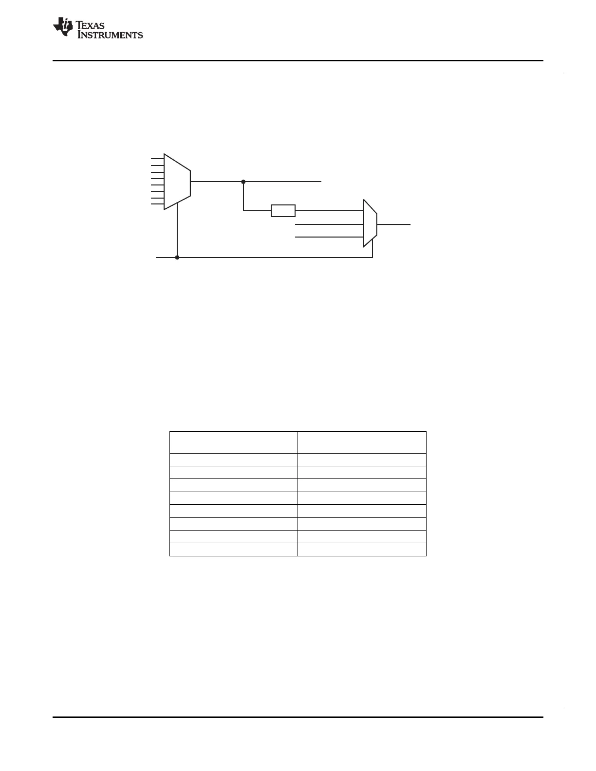
4.6.2.3 Special Clock Source Selection Scheme for VCLKA4_DIVR_EMAC
Some applications may need to use both the of Ethernet interfaces. The MII interface requires
VCLKA4_DIVR_EMAC to be 25MHz and the RMII requires VCLKA4_DIVR_EAMC to be 50MHz.
These different frequencies are supported by adding special dedicated clock source selection options for
the VCLKA4_DIVR_EMAC clock domain. This logic is shown in .
Figure 4-8. VCLKA4_DIVR Source Selection Options
The PLL2 post_ODCLK is brought out as a separate output from the PLL wrapper module. There are two
additional dividers implemented at the device-level to divide this PLL2 post_ODCLK by 8 and by 16.
As shown in , the VCLKA4_SRC configured via the system module VCLKACON1 control register is used
to determine the clock source for the VCLKA4_S and VCLKA4_DIVR. An additional multiplexor is
implemented to select between the VCLKA4_DIVR and the two additional clock sources – PLL2
post_ODCLK/8 and post_ODCLK/16.
The selection is done as shown in the following table.
Table 4-14. VCLKA4_DIVR_EMAC Clock Source
Selection
VCLKA4_SRC from Clock Source for
VCLKACON1[19–16] VCLKA4_DIVR_EMAC
0x0 OSCIN / VCLKA4R
0x1 PLL1CLK / VCLKA4R
0x2 Reserved
0x3 EXTCLKIN1 / VCLKA4R
0x4 LF LPO / VCLKA4R
0x5 HF LPO / VCLKA4R
0x6 PLL2CLK / VCLKA4R
0x7 EXTCLKIN2 / VCLKA4R
Copyright © 2012, Texas Instruments Incorporated System Information and Electrical Specifications 69
Submit Documentation Feedback
 Loading...


