13
TMS320C6748
www.ti.com
SPRS590G –JUNE 2009–REVISED JANUARY 2017
Submit Documentation Feedback
Product Folder Links: TMS320C6748
Device ComparisonCopyright © 2009–2017, Texas Instruments Incorporated
3.3.2 DSP Memory Mapping
The DSP memory map is shown in Section 3.4.
By default the DSP also has access to most on and off chip memory areas.
Additionally, the DSP megamodule includes the capability to limit access to its internal memories through
its SDMA port; without needing an external MPU unit.
3.3.2.1 External Memories
The DSP has access to the following External memories:
• Asynchronous EMIF / SDRAM / NAND / NOR Flash (EMIFA)
• SDRAM (DDR2)
3.3.2.2 DSP Internal Memories
The DSP has access to the following DSP memories:
• L2 RAM
• L1P RAM
• L1D RAM
3.3.2.3 C674x CPU
The C674x core uses a two-level cache-based architecture. The Level 1 Program cache (L1P) is 32 KB
direct mapped cache and the Level 1 Data cache (L1D) is 32 KB 2-way set associated cache. The Level 2
memory/cache (L2) consists of a 256 KB memory space that is shared between program and data space.
L2 memory can be configured as mapped memory, cache, or a combination of both.
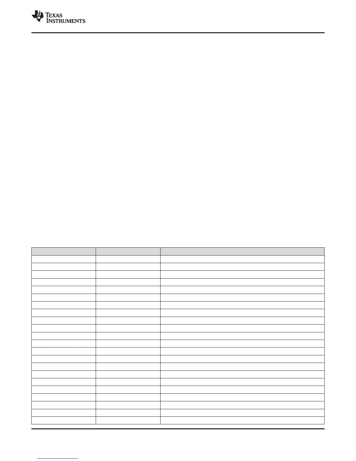
Table 3-2 shows a memory map of the C674x CPU cache registers for the device.
Table 3-2. C674x Cache Registers
Byte Address Register Name Register Description
0x0184 0000 L2CFG L2 Cache configuration register
0x0184 0020 L1PCFG L1P Size Cache configuration register
0x0184 0024 L1PCC L1P Freeze Mode Cache configuration register
0x0184 0040 L1DCFG L1D Size Cache configuration register
0x0184 0044 L1DCC L1D Freeze Mode Cache configuration register
0x0184 0048 - 0x0184 0FFC - Reserved
0x0184 1000 EDMAWEIGHT L2 EDMA access control register
0x0184 1004 - 0x0184 1FFC - Reserved
0x0184 2000 L2ALLOC0 L2 allocation register 0
0x0184 2004 L2ALLOC1 L2 allocation register 1
0x0184 2008 L2ALLOC2 L2 allocation register 2
0x0184 200C L2ALLOC3 L2 allocation register 3
0x0184 2010 - 0x0184 3FFF - Reserved
0x0184 4000 L2WBAR L2 writeback base address register
0x0184 4004 L2WWC L2 writeback word count register
0x0184 4010 L2WIBAR L2 writeback invalidate base address register
0x0184 4014 L2WIWC L2 writeback invalidate word count register
0x0184 4018 L2IBAR L2 invalidate base address register
0x0184 401C L2IWC L2 invalidate word count register
0x0184 4020 L1PIBAR L1P invalidate base address register
0x0184 4024 L1PIWC L1P invalidate word count register
0x0184 4030 L1DWIBAR L1D writeback invalidate base address register