W
V
U
T
R
P
N
M
L
K
10987654321
10987654321
DVDD3318_C
VP_CLKOUT3/
PRU1_R30[0]/
GP6[1]/
PRU1_R31[1]
SATA_VSS
SATA_RXP
VP_CLKOUT2/
MMCSD1_DAT[2]/
PRU1_R30[2]/
GP6[3]/
PRU1_R31[3]
SATA_RXN
SATA_VDD
SATA_REFCLKN
SATA_REGSATA_REFCLKP SATA_VDD
SATA_VDD SATA_VDDRSATA_VDD
DVDD3318_C
DDR_A[11]
VP_DOUT[15]/
LCD_D[15]/
UPP_XD[7]/
GP7[7]/
BOOT[7]
DV
DD3318_C
DV
DD18
DDR_DVDD18 DDR_DVDD18
DDR_D[15]
DDR_RAS
DDR_CLKP
DDR_CLKN
DDR_A[2]DDR_A[10]
V
SS
LCD_AC_ENB_CS/
GP6[0]/
PRU1_R31[28]
DDR_A[13]
DDR_CAS
DDR_A[5]
DDR_CKE
DDR_BA[0]
V
SS
CV
DD
RV
DD
DDR_A[9] DDR_A[1]
DDR_WE
DDR_D[10]
DDR_A[7]
DDR_A[0] DDR_D[12]
DDR_A[12] DDR_A[3]
DDR_CS
DDR_A[6]
DDR_DQM[1]
SATA_VSS
CV
DD
SATA_VSS
DDR_DVDD18
VP_DOUT[12]/
LCD_D[12]/
UPP_XD[4]/
GP7[4]/
BOOT[4]
DDR_VREF
DDR_BA[1]
DDR_A[8]
DDR_A[4]
DDR_BA[2]
SATA_VSS
W
V
U
T
R
P
N
M
L
K
DDR_D[13]
V
SS
V
SS
V
SS
V
SS
DV
DD18
V
SS
V
SS
V
SS
V
SS
NC
V
SS
V
SS
V
SS
V
SS
CV
DD
CV
DD
V
SS
DDR_DVDD18DDR_DVDD18DDR_DVDD18DDR_DVDD18
DVDD3318_C
VP_DOUT[13]/
LCD_D[13]/
UPP_XD[5]/
GP7[5]/
BOOT[5]
VP_DOUT[14]/
LCD_D[14]/
UPP_XD[6]/
GP7[6]/
BOOT[6]
DDR_DVDD18 DDR_DVDD18 DDR_DVDD18
VP_DOUT[9]/
LCD_D[9]/
UPP_XD[1]/
GP7[1]/
BOOT[1]
VP_DOUT[10]/
LCD_D[10]/
UPP_XD[2]/
GP7[2]/
BOOT[2]
VP_DOUT[11]/
LCD_D[11]/
UPP_XD[3]/
GP7[3]/
BOOT[3]
VP_DOUT[6]/
LCD_D[6]/
UPP_XD[14]/
GP7[14]/
PRU1_R31[14]
VP_DOUT[7]/
LCD_D[7]/
UPP_XD[15]/
GP7[15]/
PRU1_R31[15]
VP_DOUT[8]/
LCD_D[8]/
UPP_XD[0]/
GP7[0]/
BOOT[0]
VP_DOUT[3]/
LCD_D[3]/
UPP_XD[11]/
GP7[11]/
PRU1_R31[11]
VP_DOUT[4]/
LCD_D[4]/
UPP_XD[12]/
GP7[12]/
PRU1_R31[12]
VP_DOUT[5]/
LCD_D[5]/
UPP_XD[13]/
GP7[13]/
PRU1_R31[13]
VP_DOUT[0]/
LCD_D[0]/
UPP_XD[8]/
GP7[8]/
PRU1_R31[8]
VP_DOUT[1]/
LCD_D[1]/
UPP_XD[9]/
GP7[9]/
PRU1_R31[9]
VP_DOUT[2]/
LCD_D[2]/
UPP_XD[10]/
GP7[10]/
PRU1_R31[10]
23
TMS320C6748
www.ti.com
SPRS590G –JUNE 2009–REVISED JANUARY 2017
Submit Documentation Feedback
Product Folder Links: TMS320C6748
Device ComparisonCopyright © 2009–2017, Texas Instruments Incorporated
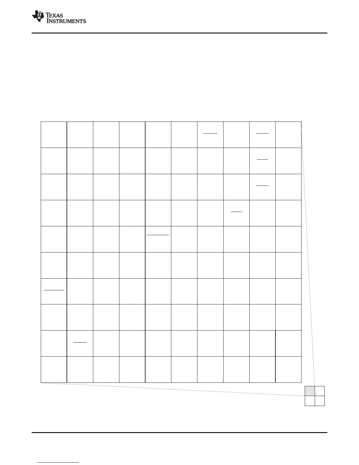
3.5 Pin Assignments
Extensive use of pin multiplexing is used to accommodate the largest number of peripheral functions in
the smallest possible package. Pin multiplexing is controlled using a combination of hardware
configuration at device reset and software programmable register settings.
3.5.1 Pin Map (Bottom View)
The following graphics show the bottom view of the ZCE and ZWT packages pin assignments in four
quadrants (A, B, C, and D). The pin assignments for both packages are identical.
Figure 3-3. Pin Map (Quad A)