8
TMS320C6748
SPRS590G –JUNE 2009–REVISED JANUARY 2017
www.ti.com
Submit Documentation Feedback
Product Folder Links: TMS320C6748
Device Comparison Copyright © 2009–2017, Texas Instruments Incorporated
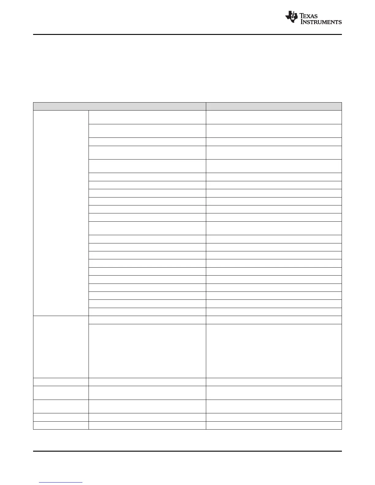
3 Device Comparison
3.1 Device Characteristics
Table 3-1 provides an overview of the device. The table shows significant features of the device, including
the capacity of on-chip RAM, peripherals, and the package type with pin count.
Table 3-1. Characteristics of C6748
HARDWARE FEATURES C6748
Peripherals
Not all peripherals pins
are available at the
same time (for more
detail, see the Device
Configurations section).
DDR2/mDDR Memory Controller
DDR2, 16-bit bus width, up to 156 MHz
Mobile DDR, 16-bit bus width, up to 150 MHz
EMIFA
Asynchronous (8/16-bit bus width) RAM, Flash,
16-bit SDRAM, NOR, NAND
Flash Card Interface 2 MMC and SD cards supported
EDMA3
64 independent channels, 16 QDMA channels,
2 channel controllers, 3 transfer controllers
Timers
4 64-Bit General Purpose (each configurable as 2 separate
32-bit timers, one configurable as Watch Dog)
UART 3 (each with RTS and CTS flow control)
SPI 2 (Each with one hardware chip select)
I
2
C 2 (both Master/Slave)
Multichannel Audio Serial Port [McASP] 1 (each with transmit/receive, FIFO buffer, 16 serializers)
Multichannel Buffered Serial Port [McBSP] 2 (each with transmit/receive, FIFO buffer, 16)
10/100 Ethernet MAC with Management Data I/O 1 (MII or RMII Interface)
eHRPWM
4 Single Edge, 4 Dual Edge Symmetric, or
2 Dual Edge Asymmetric Outputs
eCAP 3 32-bit capture inputs or 3 32-bit auxiliary PWM outputs
UHPI 1 (16-bit multiplexed address/data)
USB 2.0 (USB0) High-Speed OTG Controller with on-chip OTG PHY
USB 1.1 (USB1) Full-Speed OHCI (as host) with on-chip PHY
General-Purpose Input/Output Port 9 banks of 16-bit
LCD Controller 1
SATA Controller 1 (Supports both SATA I and SATAII)
Universal Parallel Port (uPP) 1
Video Port Interface (VPIF) 1 (video in and video out)
PRU Subsystem (PRUSS) 2 Programmable PRU Cores
On-Chip Memory
Size (Bytes) 448KB RAM
Organization
DSP
32KB L1 Program (L1P)/Cache (up to 32KB)
32KB L1 Data (L1D)/Cache (up to 32KB)
256KB Unified Mapped RAM/Cache (L2)
DSP Memories can be made accessible to EDMA3 and
other peripherals.
ADDITIONAL MEMORY
128KB RAM
Security Secure Boot TI Basic Secure Boot
C674x CPU ID + CPU
Rev ID
Control Status Register (CSR.[31:16]) 0x1400
C674x Megamodule
Revision
Revision ID Register (MM_REVID[15:0]) 0x0000
JTAG BSDL_ID DEVIDR0 Register see Section 6.34.4.1, JTAG Peripheral Register Description
CPU Frequency MHz 674x DSP 375 MHz (1.2V) or 456 MHz (1.3V)