27
TMS320C6748
www.ti.com
SPRS590G –JUNE 2009–REVISED JANUARY 2017
Submit Documentation Feedback
Product Folder Links: TMS320C6748
Device ComparisonCopyright © 2009–2017, Texas Instruments Incorporated
(1) I = Input, O = Output, I/O = Bidirectional, Z = High impedance, PWR = Supply voltage, GND = Ground, A = Analog signal.
Note: For multiplexed pins where functions have different types (ie., input versus output), the table reflects the pin function direction for
that particular peripheral.
(2) IPD = Internal Pulldown resistor, IPU = Internal Pullup resistor. CP[n] = configurable pull-up/pull-down (where n is the pin group) using
the PUPDENA and PUPDSEL registers in the System Module. For more detailed information on pullup/pulldown resistors and situations
where external pullup/pulldown resistors are required, see the Device Configuration section. For electrical specifications on pullup and
internal pulldown circuits, see the Device Operating Conditions section.
(3) This signal is part of a dual-voltage IO group (A, B or C). These groups can be operated at 3.3V or 1.8V nominal. The three groups can
be operated at independent voltages but all pins withina group will operate at the same voltage. Group A operates at the voltage of
power supply DVDD3318_A. Group B operates at the voltage of power supply DVDD3318_B. Group C operates at the voltage of power
supply DVDD3318_C.
(4) Open drain mode for RESETOUT function.
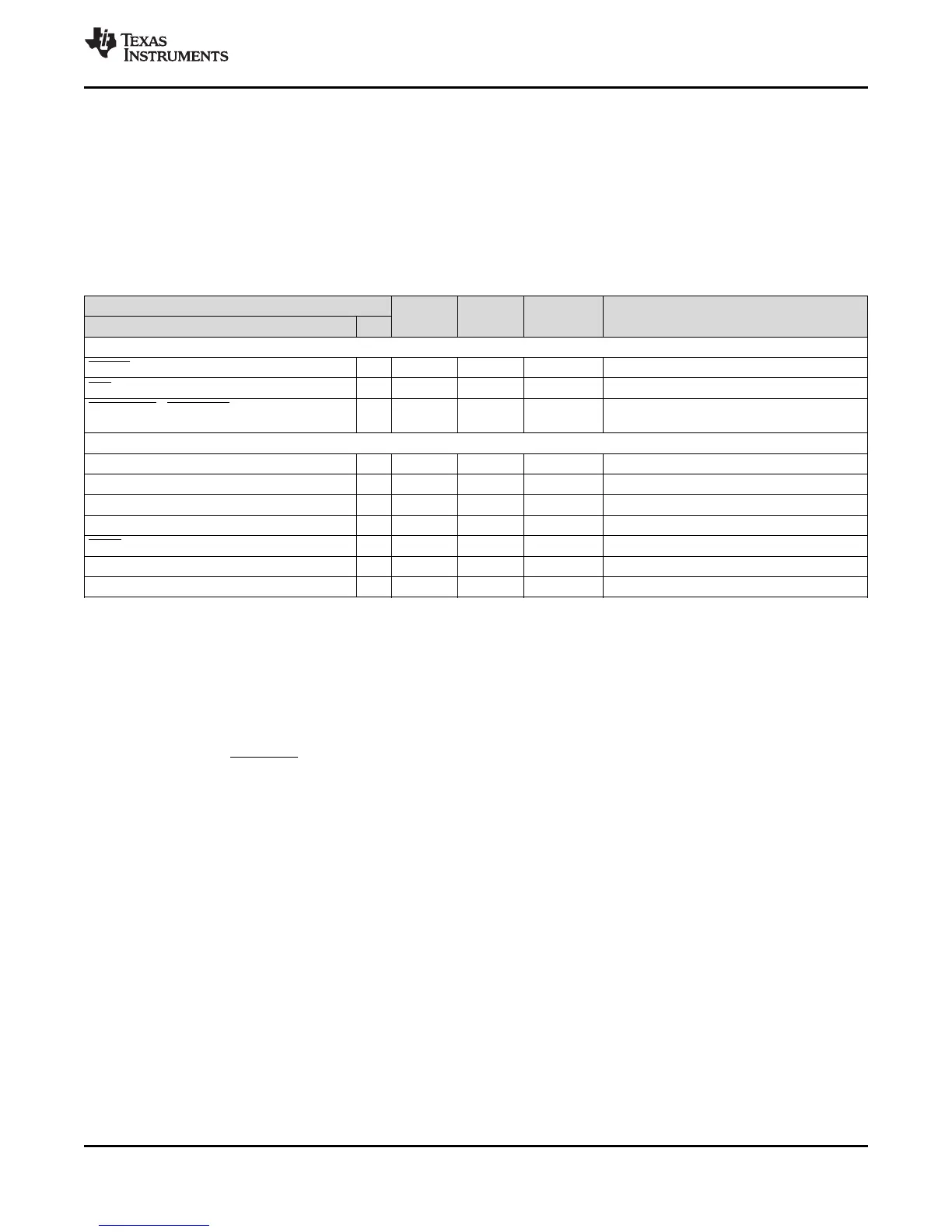
3.7 Terminal Functions
Table 3-5 to Table 3-31 identify the external signal names, the associated pin/ball numbers along with the
mechanical package designator, the pin type (I, O, IO, OZ, or PWR), whether the pin/ball has any internal
pullup/pulldown resistors, whether the pin/ball is configurable as an IO in GPIO mode, and a functional pin
description.
3.7.1 Device Reset, NMI and JTAG
Table 3-5. Reset, NMI and JTAG Terminal Functions
SIGNAL
TYPE
(1)
PULL
(2)
POWER
GROUP
(3)
DESCRIPTION
NAME NO.
RESET
RESET K14 I — B Device reset input
NMI J17 I IPU B Non-Maskable Interrupt
RESETOUT / UHPI_HAS / PRU1_R30[14] /
GP6[15]
T17 O
(4)
CP[21] C Reset output
JTAG
TMS L16 I IPU B JTAG test mode select
TDI M16 I IPU B JTAG test data input
TDO J18 O IPU B JTAG test data output
TCK J15 I IPU B JTAG test clock
TRST L17 I IPD B JTAG test reset
EMU0 J16 I/O IPU B Emulation pin
EMU1 K16 I/O IPU B Emulation pin