OSCOUT
OSCIN
OSCV
SS
Clock
Input
toPLL
NC
87
TMS320C6748
www.ti.com
SPRS590G –JUNE 2009–REVISED JANUARY 2017
Submit Documentation Feedback
Product Folder Links: TMS320C6748
Peripheral Information and Electrical SpecificationsCopyright © 2009–2017, Texas Instruments Incorporated
(1) Whichever is smaller. P = the period of the applied signal. Maintaining transition times as fast as possible is recommended to improve
noise immunity on input signals.
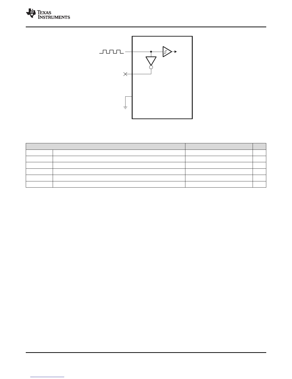
Figure 6-7. External 1.2V Clock Source
Table 6-3. OSCIN Timing Requirements for an Externally Driven Clock
PARAMETER MIN MAX UNIT
f
OSCIN
OSCIN frequency range 12 50 MHz
t
c(OSCIN)
Cycle time, external clock driven on OSCIN 20 ns
t
w(OSCINH)
Pulse width high, external clock on OSCIN 0.4 t
c(OSCIN)
ns
t
w(OSCINL)
Pulse width low, external clock on OSCIN 0.4 t
c(OSCIN)
ns
t
t(OSCIN)
Transition time, OSCIN 0.25P or 10
(1)
ns
t
j(OSCIN)
Period jitter, OSCIN 0.02P ns
6.6 Clock PLLs
The device has two PLL controllers that provide clocks to different parts of the system. PLL0 provides
clocks (though various dividers) to most of the components of the device. PLL1 provides clocks to the
DDR2/mDDR Controller and provides an alternate clock source for the ASYNC3 clock domain. This allows
the peripherals on the ASYNC3 clock domain to be immune to frequency scaling operation on PLL0.
The PLL controller provides the following:
• Glitch-Free Transitions (on changing clock settings)
• Domain Clocks Alignment
• Clock Gating
• PLL power down
The various clock outputs given by the controller are as follows:
• Domain Clocks: SYSCLK [1:n]
• Auxiliary Clock from reference clock source: AUXCLK
Various dividers that can be used are as follows:
• Post-PLL Divider: POSTDIV
• SYSCLK Divider: D1, ¼, Dn
Various other controls supported are as follows:
• PLL Multiplier Control: PLLM
• Software programmable PLL Bypass: PLLEN