0.1
µF
0.01
µF
50R
1.14V - 1.32V
50RV
SS
PLL1_VDDA
PLL1_VSSA
Ferrite Bead: Murata BLM31PG500SN1L or Equivalent
0.1
µF
0.01
µF
50R
1.14V - 1.32V
50RV
SS
PLL0_VDDA
PLL0_VSSA
88
TMS320C6748
SPRS590G –JUNE 2009–REVISED JANUARY 2017
www.ti.com
Submit Documentation Feedback
Product Folder Links: TMS320C6748
Peripheral Information and Electrical Specifications Copyright © 2009–2017, Texas Instruments Incorporated
6.6.1 PLL Device-Specific Information
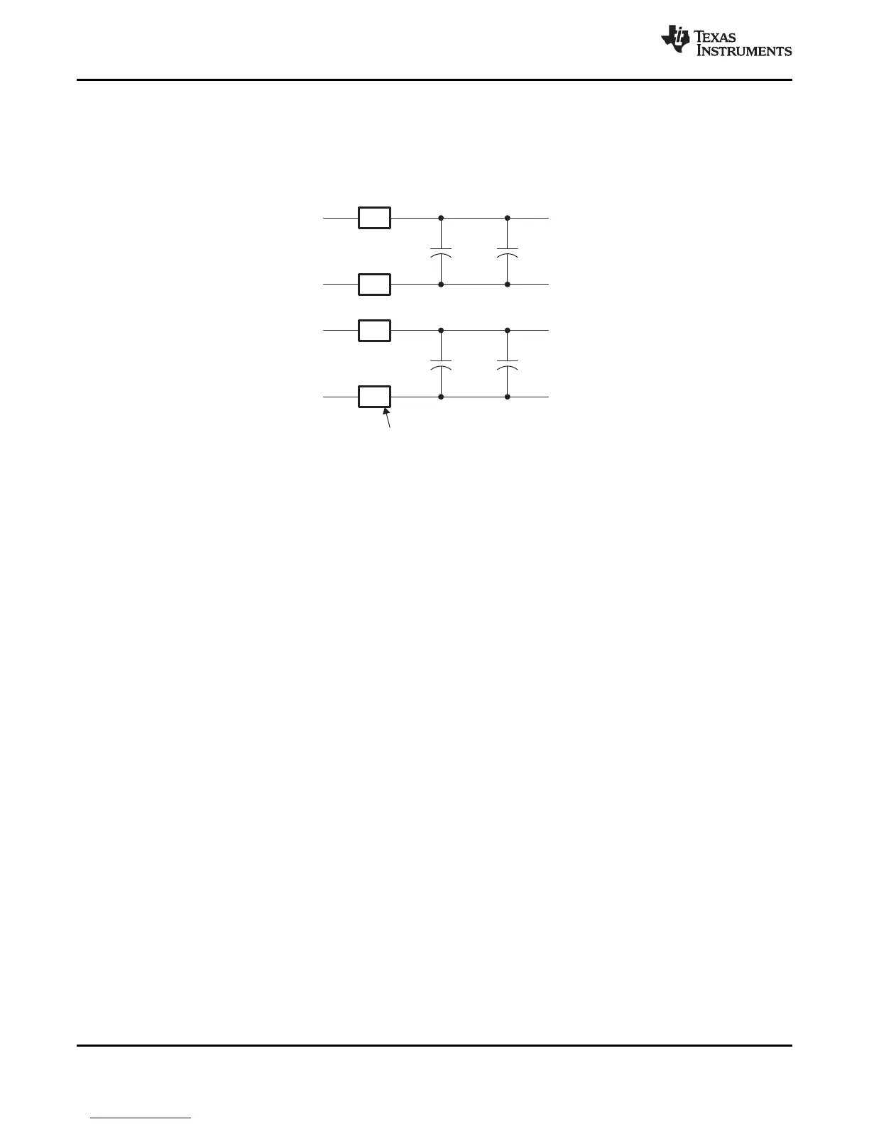
The device DSP generates the high-frequency internal clocks it requires through an on-chip PLL.
The PLL requires some external filtering components to reduce power supply noise as shown in Figure 6-
8.
Figure 6-8. PLL External Filtering Components
The external filtering components shown above provide noise immunity for the PLLs. PLL0_VDDA and
PLL1_VDDA should not be connected together to provide noise immunity between the two PLLs.
Likewise, PLL0_VSSA and PLL1_VSSA should not be connected together.
The input to the PLL is either from the on-chip oscillator or from an external clock on the OSCIN pin. PLL0
outputs seven clocks that have programmable divider options. PLL1 outputs three clocks that have
programmable divider options. Figure 6-9 illustrates the high-level view of the PLL Topology.
The PLLs are disabled by default after a device reset. They must be configured by software according to
the allowable operating conditions listed in Table 6-4 before enabling the device to run from the PLL by
setting PLLEN = 1.