Switched Central Resource (SCR)
BOOT ROM
256KB L2 RAM
32KB
L1 RAM
32KB
L1 Pgm
AET
C674x™
DSP CPU
DSP Subsystem
JTAG Interface
System Control
Input
Clock(s)
Power/Sleep
Controller
Pin
Multiplexing
PLL/Clock
Generator
w/OSC
General-
Purpose
Timer (x3)
Serial Interfaces
Audio Ports
McASP
w/FIFO
DMA
Peripherals
Display Internal Memory
LCD
Ctlr
128KB
RAM
External Memory InterfacesConnectivity
EDMA3
(x2)
Control Timers
ePWM
(x2)
eCAP
(x3)
EMIFA(8b/16B)
NAND/Flash
16b SDRAM
DDR2/MDDR
Controller
RTC/
32-kHz
OSC
I C
(x2)
2
SPI
(x2)
UART
(x3)
McBSP
(x2)
Video
VPIF
Parallel Port
uPP
EMAC
10/100
(MII/RMII)
MDIO
USB1.1
OHCI Ctlr
PHY
USB2.0
OTG Ctlr
PHY
HPI
MMC/SD
(8b)
(x2)
SATA
Customizable Interface
PRU Subsystem
Memory
Protection
5
TMS320C6748
www.ti.com
SPRS590G –JUNE 2009–REVISED JANUARY 2017
Submit Documentation Feedback
Product Folder Links: TMS320C6748
Device OverviewCopyright © 2009–2017, Texas Instruments Incorporated
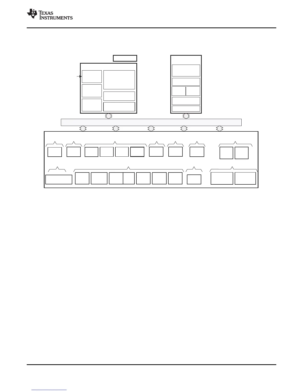
1.4 Functional Block Diagram
Figure 1-1 shows the functional block diagram of the device.
Figure 1-1. Functional Block Diagram