119
TMS320C6748
www.ti.com
SPRS590G –JUNE 2009–REVISED JANUARY 2017
Submit Documentation Feedback
Product Folder Links: TMS320C6748
Peripheral Information and Electrical SpecificationsCopyright © 2009–2017, Texas Instruments Incorporated
(1) DDR2 is not supported at this voltage operating point.
6.11 DDR2/mDDR Memory Controller
The DDR2/mDDR Memory Controller is a dedicated interface to DDR2/mDDR SDRAM. It supports
JESD79-2A standard compliant DDR2 SDRAM devices and compliant Mobile DDR SDRAM devices.
The DDR2/mDDR Memory Controller support the following features:
• JESD79-2A standard compliant DDR2 SDRAM
• Mobile DDR SDRAM
• 256 MByte memory space for DDR2
• 256 MByte memory space for mDDR
• CAS latencies:
– DDR2: 2, 3, 4 and 5
– mDDR: 2 and 3
• Internal banks:
– DDR2: 1, 2, 4 and 8
– mDDR:1, 2 and 4
• Burst length: 8
• Burst type: sequential
• 1 chip select (CS) signal
• Page sizes: 256, 512, 1024, and 2048
• SDRAM autoinitialization
• Self-refresh mode
• Partial array self-refresh (for mDDR)
• Power down mode
• Prioritized refresh
• Programmable refresh rate and backlog counter
• Programmable timing parameters
• Little endian
6.11.1 DDR2/mDDR Memory Controller Electrical Data/Timing
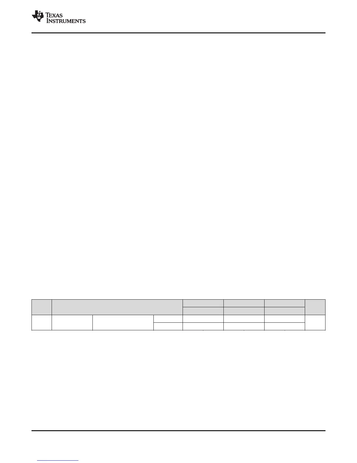
Table 6-23. Switching Characteristics Over Recommended Operating Conditions for DDR2/mDDR
Memory Controller
No. PARAMETER 1.3V, 1.2V 1.1V 1.0V UNIT
MIN MAX MIN MAX MIN MAX
1 t
c(DDR_CLK)
Cycle time,
DDR_CLKP / DDR_CLKN
DDR2 125 156 125 150 —
(1)
—
(1)
MHz
mDDR 105 150 100 133 95 133
 Loading...