120
TMS320C6748
SPRS590G –JUNE 2009–REVISED JANUARY 2017
www.ti.com
Submit Documentation Feedback
Product Folder Links: TMS320C6748
Peripheral Information and Electrical Specifications Copyright © 2009–2017, Texas Instruments Incorporated
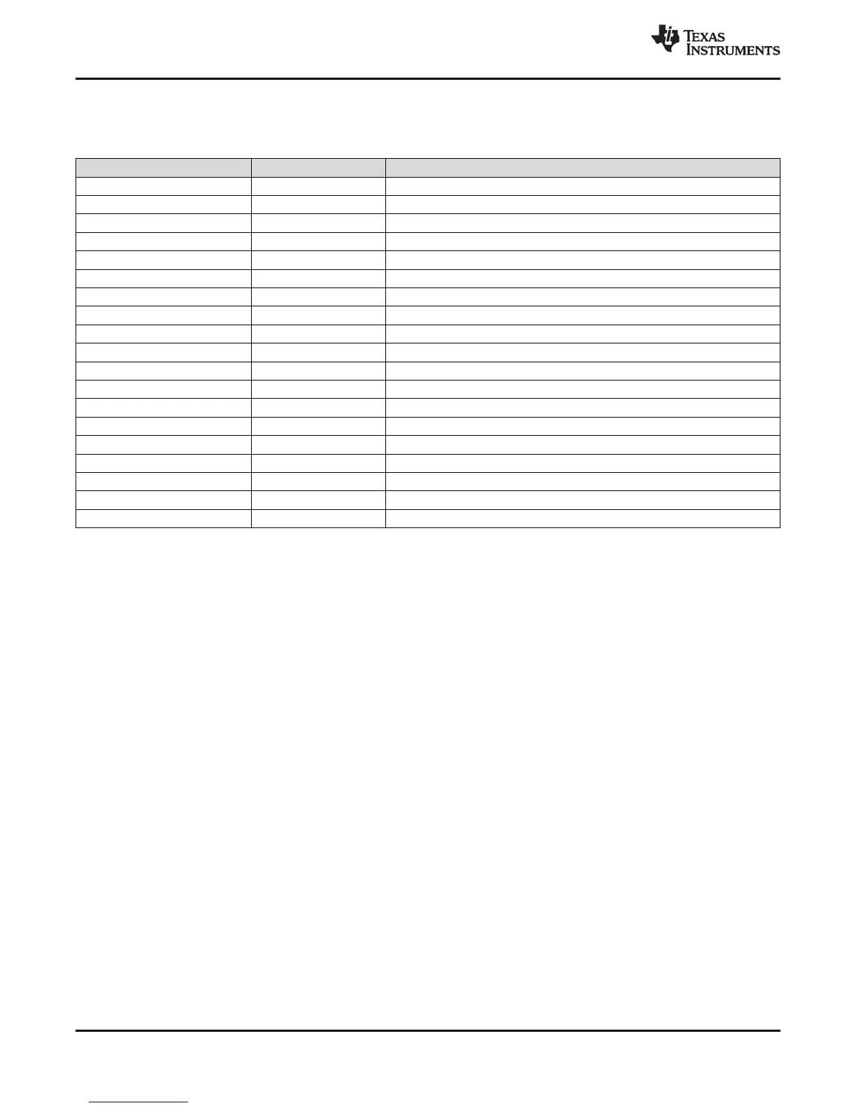
6.11.2 DDR2/mDDR Memory Controller Register Description(s)
Table 6-24. DDR2/mDDR Memory Controller Registers
BYTE ADDRESS ACRONYM REGISTER DESCRIPTION
0xB000 0000 REVID Revision ID Register
0xB000 0004 SDRSTAT SDRAM Status Register
0xB000 0008 SDCR SDRAM Configuration Register
0xB000 000C SDRCR SDRAM Refresh Control Register
0xB000 0010 SDTIMR1 SDRAM Timing Register 1
0xB000 0014 SDTIMR2 SDRAM Timing Register 2
0xB000 001C SDCR2 SDRAM Configuration Register 2
0xB000 0020 PBBPR Peripheral Bus Burst Priority Register
0xB000 0040 PC1 Performance Counter 1 Registers
0xB000 0044 PC2 Performance Counter 2 Register
0xB000 0048 PCC Performance Counter Configuration Register
0xB000 004C PCMRS Performance Counter Master Region Select Register
0xB000 0050 PCT Performance Counter Time Register
0xB000 00C0 IRR Interrupt Raw Register
0xB000 00C4 IMR Interrupt Mask Register
0xB000 00C8 IMSR Interrupt Mask Set Register
0xB000 00CC IMCR Interrupt Mask Clear Register
0xB000 00E4 DRPYC1R DDR PHY Control Register 1
0x01E2 C000 VTPIO_CTL VTP IO Control Register
6.11.3 DDR2/mDDR Interface
This section provides the timing specification for the DDR2/mDDR interface as a PCB design and
manufacturing specification. The design rules constrain PCB trace length, PCB trace skew, signal
integrity, cross-talk, and signal timing. These rules, when followed, result in a reliable DDR2/mDDR
memory system without the need for a complex timing closure process. For more information regarding
guidelines for using this DDR2/mDDR specification, Understanding TI's PCB Routing Rule-Based DDR2
Timing Specification (SPRAAV0).
6.11.3.1 DDR2/mDDR Interface Schematic
Figure 6-18 shows the DDR2/mDDR interface schematic for a single-memory DDR2/mDDR system. The
dual-memory system shown in Figure 6-19. Pin numbers for the device can be obtained from the pin
description section.
 Loading...


