EasyManua.ls Logo

Texas Instruments TMS320C6748 User Manual

Texas Instruments TMS320C6748
274 pages
To Next Page IconTo Next Page
To Previous Page IconTo Previous Page
Page #26 background image
J
H
G
F
E
D
C
B
A
10987654321
10987654321
EMA_D[15]/
GP3[7]
AXR15/
EPWM0TZ[0]/
ECAP2_APWM2/
GP0[7]
ACLKR/
PRU0_R30[20]/
GP0[15]/
PRU0_R31[22]
ACLKX/
PRU0_R30[19]/
GP0[14]/
PRU0_R31[21]
AHCLKX/
USB_REFCLKIN/
/
GP0[10]/
PRU0_R31[17]
UART1_CTS
AFSX/
GP0[12]/
PRU0_R31[19]
AFSR/
GP0[13]/
PRU0_R31[20]
AXR9/
DX1/
GP0[1]
AXR4/
FSR0/
GP1[12]/
MII_COL
AXR5/
CLKX0/
GP1[13]/
MII_TXCLK
AXR7/
EPWM1TZ[0]/
PRU0_R30[17]
GP1[15]/
PRU0_R31[7]
AXR10/
DR1/
GP0[2]
AXR1/
DX0/
GP1[9]/
MII_TXD[1]
AXR3/
FSX0/
GP1[11]/
MII_TXD[3]
AXR2/
DR0/
GP1[10]/
MII_TXD[2]
MMCSD1_DAT[6]/
LCD_MCLK/
PRU1_R30[6]/
GP8[10]/
PRU1_R31[7]
RTC_ALARM/
/
GP0[8]/
UART2_CTS
DEEPSLEEP
AXR0/
ECAP0_APWM0/
GP8[7]/
MII_TXD[0]/
CLKS0
PRU0_R30[24]/
MMCSD1_CLK/
UPP_CHB_START/
GP8[14]/
PRU1_R31[26]
MMCSD1_DAT[4]/
LCD_VSYNC/
PRU1_R30[4]/
GP8[8]/
PRU1_R31[5]
SATA_VSS
PRU0_R30[22]/
PRU1_R30[8]/
UPP_CHB_WAIT/
GP8[12]/
PRU1_R31[24]
AXR8/
CLKS1/
ECAP1_APWM1/
GP0[0]/
PRU0_R31[8]
AXR12/
FSR1/
GP0[4]
EMA_D[4]/
GP4[12]
AXR14/
CLKR1/
GP0[6]
EMA_WEN_DQM[1]/
GP2[2]
EMA_D[0]/
GP4[8]
EMA_A[19]/
MMCSD0_DAT[2]/
PRU1_R30[27]/
GP4[3]
EMA_D[9]/
GP3[1]
EMA_A_R /
GP3[9]
W
MMCSD0_CLK/
PRU1_R30[31]/
GP4[7]
EMA_D[8]/
GP3[0]
EMA_D[13]/
GP3[5]
VP_CLKIN2/
MMCSD1_DAT[3]/
PRU1_R30[3]/
GP6[4]/
PRU1_R31[4]
VP_CLKIN3/
MMCSD1_DAT[1]/
PRU1_R30[1]/
GP6[2]/
PRU1_R31[2]
AMUTE/
GP0[9]/
PRU0_R31[16]
PRU0_R30[16]/
UART2_RTS/
DV
DD3318_A
DV
DD3318_A
EMA_WE/
GP3[11]
EMA_D[10]/
GP3[2]
EMA_D[3]/
GP4[11]
EMA_SDCKE/
PRU0_R30[4]/
GP2[6]/
PRU0_R31[4]
EMA_D[14]/
GP3[6]
EMA_D[7]/
GP4[15]
EMA_D[1]/
GP4[9]
EMA_A[22]/
MMCSD0_CMD/
PRU1_R30[30]/
GP4[6]
EMA_D[2]/
GP4[10]
EMA_A[21]/
MMCSD0_DAT[0]/
PRU1_R30[29]/
GP4[5]
PRU0_R30[23]/
MMCSD1_CMD/
UPP_CHB_ENABLE/
GP8[13]/
PRU1_R31[25]
AHCLKR/
/
GP0[11]/
PRU0_R31[18]
PRU0_R30[18]/
UART1_RTS
EMA_D[12]/
GP3[4]
EMA_WEN_DQM[0]/
GP2[3]
EMA_CLK/
PRU0_R30[5]/
GP2[7]/
PRU0_R31[5]
AXR6/
CLKR0/
GP1[14]/
MII_TXEN/
PRU0_R31[6]
AXR11/
FSX1/
GP0[3]
EMA_D[6]/
GP4[14]
EMA_D[11]/
GP3[3]
RV
DD
EMA_D[5]/
GP4[13]
MMCSD1_DAT[7]/
LCD_PCLK/
PRU1_R30[7]/
GP8[11]
MMCSD1_DAT[5]/
LCD_HSYNC/
PRU1_R30[5]/
GP8[9]/
PRU1_R31[6]
PRU0_R30[25]/
MMCSD1_DAT[0]/
UPP_CHB_CLOCK/
GP8[15]/
PRU1_R31[27]
AXR13/
CLKX1/
GP0[5]
J
H
G
F
E
D
C
B
A
EMA_CS[4]/
GP3[13]
EMA_CAS/
PRU0_R30[2]/
GP2[4]/
PRU0_R31[2]
DV
DD3318_B
DV
DD3318_B
DV
DD3318_B
DV
DD3318_B
DV
DD18
CV
DD
CV
DD
DV
DD3318_B
DV
DD18
SATA_VSS
DV
DD3318_A
V
SS
V
SS
CV
DD
CV
DD
V
SS
V
SS
CV
DD
SATA_TXP
SATA_TXN
DV
DD3318_C
CV
DD
V
SS
V
SS
26
TMS320C6748
SPRS590G JUNE 2009REVISED JANUARY 2017
www.ti.com
Submit Documentation Feedback
Product Folder Links: TMS320C6748
Device Comparison Copyright © 2009–2017, Texas Instruments Incorporated
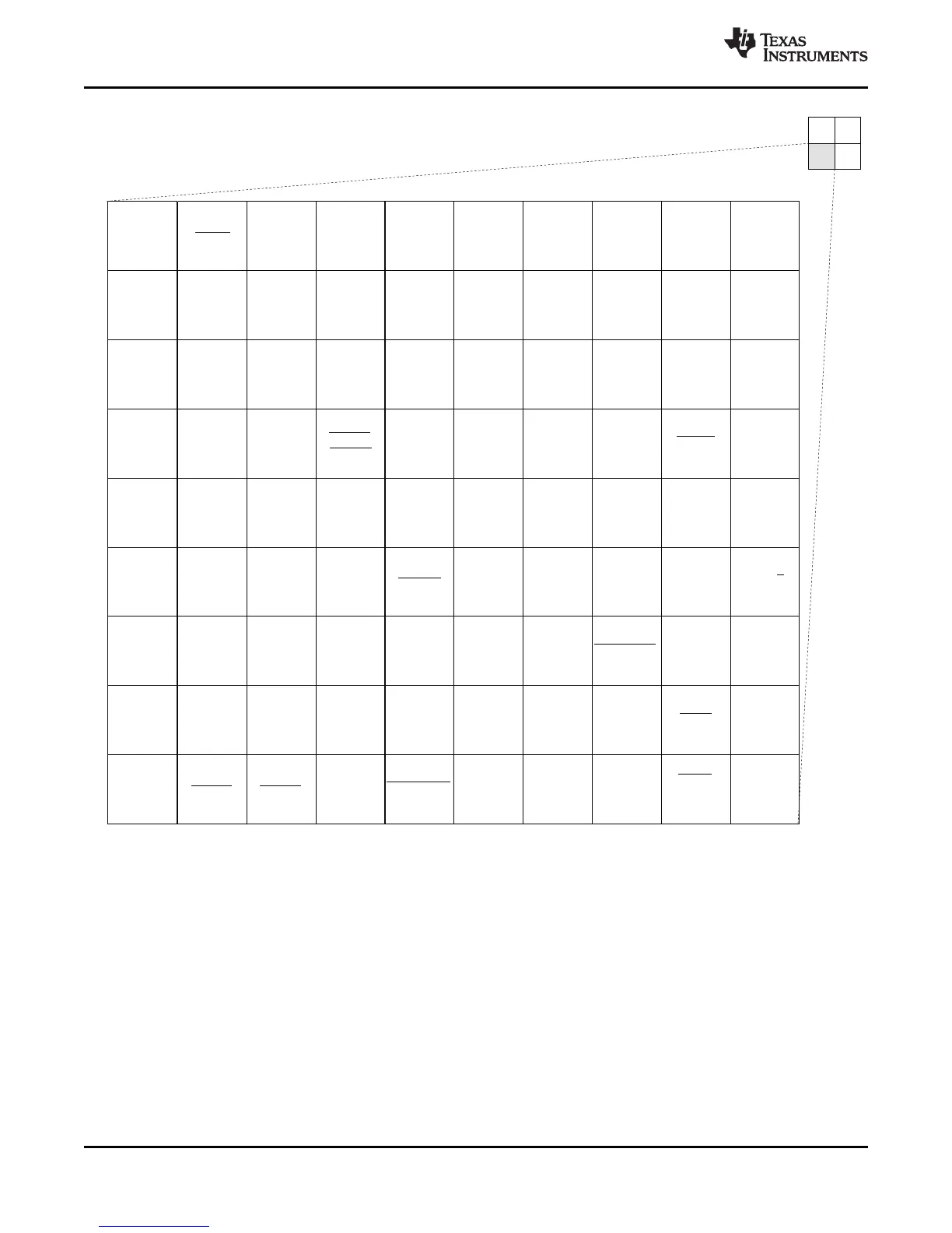
Figure 3-6. Pin Map (Quad D)
3.6 Pin Multiplexing Control
Device level pin multiplexing is controlled by registers PINMUX0 - PINMUX19 in the SYSCFG module.
For the device family, pin multiplexing can be controlled on a pin-by-pin basis. Each pin that is multiplexed
with several different functions has a corresponding 4-bit field in one of the PINMUX registers.
Pin multiplexing selects which of several peripheral pin functions controls the pin's IO buffer output data
and output enable values only. The default pin multiplexing control for almost every pin is to select 'none'
of the peripheral functions in which case the pin's IO buffer is held tri-stated.
Note that the input from each pin is always routed to all of the peripherals that share the pin; the PINMUX
registers have no effect on input from a pin.

Table of Contents

Question and Answer IconNeed help?

Do you have a question about the Texas Instruments TMS320C6748 and is the answer not in the manual?

Texas Instruments TMS320C6748 Specifications

General IconGeneral
BrandTexas Instruments
ModelTMS320C6748
CategoryControl Unit
LanguageEnglish

Summary

Device Overview

Features

Lists the key features of the TMS320C674x Fixed- and Floating-Point VLIW DSP.

Description

Functional Block Diagram

Device Comparison

Device Characteristics

Overview of C6748 hardware features, peripherals, on-chip memory, and package type.

Memory Map Summary

Pin Assignments

Pin Multiplexing Control

Terminal Functions

Device Reset, NMI and JTAG Terminal Functions

Details terminal functions for RESET, NMI, and JTAG signals.

External Memory Interface A (EMIFA) Terminal Functions

Details terminal functions for the External Memory Interface A.

DDR2/mDDR Controller Terminal Functions

Details terminal functions for the DDR2/mDDR Memory Controller.

Serial Peripheral Interface Modules (SPI) Terminal Functions

Details terminal functions for SPI0 and SPI1 modules.

Programmable Real-Time Unit (PRU) Terminal Functions

Details terminal functions for the Programmable Real-Time Unit.

Boot

Details boot mode selection terminal functions.

Inter-Integrated Circuit Modules(I2C0, I2C1) Terminal Functions

Details terminal functions for I2C0 and I2C1 modules.

Multichannel Audio Serial Ports (McASP) Terminal Functions

Details terminal functions for McASP modules.

Multichannel Buffered Serial Ports (McBSP) Terminal Functions

Details terminal functions for McBSP modules.

Universal Serial Bus Modules (USB0, USB1) Terminal Functions

Details terminal functions for USB0 and USB1 modules.

Ethernet Media Access Controller (EMAC) Terminal Functions

Details terminal functions for the EMAC module.

Multimedia Card/Secure Digital (MMC/SD) Terminal Functions

Details terminal functions for MMC/SD card interfaces.

Liquid Crystal Display Controller(LCD) Terminal Functions

Details terminal functions for the LCD controller.

Serial ATA Controller (SATA) Terminal Functions

Details terminal functions for the SATA controller.

Universal Host-Port Interface (UHPI) Terminal Functions

Details terminal functions for the UHPI interface.

Universal Parallel Port (uPP) Terminal Functions

Details terminal functions for the Universal Parallel Port.

Video Port Interface (VPIF) Terminal Functions

Details terminal functions for the Video Port Interface.

Supply and Ground Terminal Functions

Details terminal functions for supply and ground pins.

Device Configuration

Boot Modes

Describes the various boot modes supported by the internal DSP ROM bootloader.

Pullup/Pulldown Resistors

Specifications

Absolute Maximum Ratings Over Operating Junction Temperature Range

Specifies the absolute maximum ratings for voltage and temperature.

Handling Ratings

Details handling precautions, including ESD voltage ratings.

Recommended Operating Conditions

Specifies recommended operating conditions for supply voltage and junction temperature.

Electrical Characteristics Over Recommended Ranges of Supply Voltage and Operating Junction Temperature

Details electrical characteristics over recommended operating ranges.

Power Supplies

Power-On Sequence

Describes the required order for powering on the device's various supplies.

Reset

Power-On Reset (POR)

Explains the Power-On Reset behavior and its effects on device logic and pins.

Reset Electrical Data Timings

Crystal Oscillator or External Clock Input

Clock PLLs

Enhanced Direct Memory Access Controller (EDMA3)

EDMA3 Peripheral Register Descriptions

Describes the EDMA3 Channel Controller and Transfer Controller registers.

Interrupts

DSP Interrupts

Details the C674x DSP interrupt controller, prioritized interrupts, and registers.

Power and Sleep Controller (PSC)

Memory Protection Units

MMC / SD / SDIO (MMCSD0, MMCSD1)

Serial ATA Controller (SATA)

Multichannel Audio Serial Port (McASP)

Multichannel Buffered Serial Port (McBSP)

Serial Peripheral Interface Ports (SPI0, SPI1)

Inter-Integrated Circuit Serial Ports (I2C)

Universal Asynchronous Receiver/Transmitter (UART)

Universal Serial Bus OTG Controller (USB0) [USB2.0 OTG]

Universal Serial Bus Host Controller (USB1) [USB1.1 OHCI]

Ethernet Media Access Controller (EMAC)

LCD Controller (LCDC)

Host-Port Interface (UHPI)

Universal Parallel Port (uPP)

Video Port Interface (VPIF)

Enhanced Capture (eCAP) Peripheral

Real Time Clock (RTC)

General-Purpose Input/Output (GPIO)

Programmable Real-Time Unit Subsystem (PRUSS)

Emulation Logic

Electrostatic Discharge Caution

Related product manuals