164
TMS320C6748
SPRS590G –JUNE 2009–REVISED JANUARY 2017
www.ti.com
Submit Documentation Feedback
Product Folder Links: TMS320C6748
Peripheral Information and Electrical Specifications Copyright © 2009–2017, Texas Instruments Incorporated
6.17.2 SPI Electrical Data/Timing
6.17.2.1 Serial Peripheral Interface (SPI) Timing
Table 6-68 through Table 6-83 assume testing over recommended operating conditions (see Figure 6-38
through Figure 6-41).
(1) P = SYSCLK2 period; M = t
c(SPC)M
(SPI master bit clock period)
(2) This timing is limited by the timing shown or 3P, whichever is greater.
(3) First bit may be MSB or LSB depending upon SPI configuration. MO(0) refers to first bit and MO(n) refers to last bit output on
SPI0_SIMO. MI(0) refers to the first bit input and MI(n) refers to the last bit input on SPI0_SOMI.
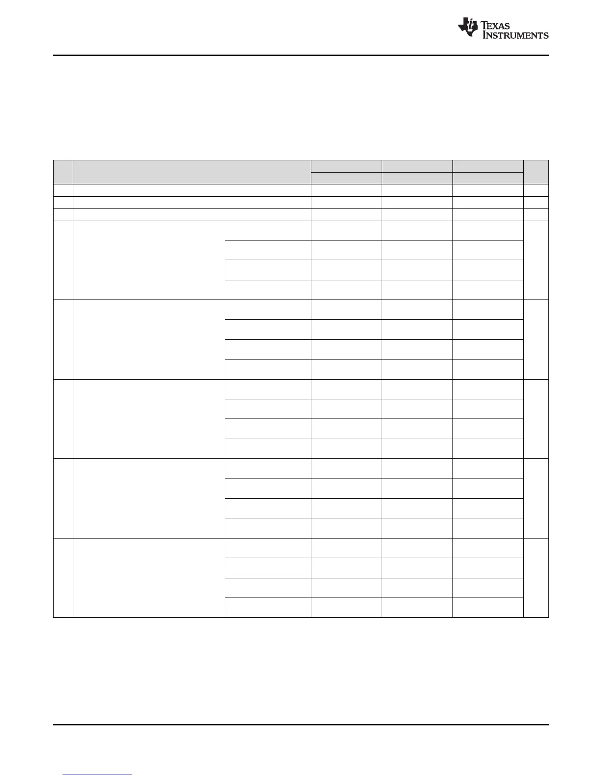
Table 6-68. General Timing Requirements for SPI0 Master Modes
(1)
NO.
1.3V, 1.2V 1.1V 1.0V
UNIT
MIN MAX MIN MAX MIN MAX
1 t
c(SPC)M
Cycle Time, SPI0_CLK, All Master Modes 20
(2)
256P 30
(2)
256P 40
(2)
256P ns
2 t
w(SPCH)M
Pulse Width High, SPI0_CLK, All Master Modes 0.5M-1 0.5M-1 0.5M-1 ns
3 t
w(SPCL)M
Pulse Width Low, SPI0_CLK, All Master Modes 0.5M-1 0.5M-1 0.5M-1 ns
4 t
d(SIMO_SPC)M
Delay, initial data bit valid on
SPI0_SIMO after initial edge
on SPI0_CLK
(3)
Polarity = 0, Phase = 0,
to SPI0_CLK rising
5 5 6
ns
Polarity = 0, Phase = 1,
to SPI0_CLK rising
-0.5M+5 -0.5M+5 -0.5M+6
Polarity = 1, Phase = 0,
to SPI0_CLK falling
5 5 6
Polarity = 1, Phase = 1,
to SPI0_CLK falling
-0.5M+5 -0.5M+5 -0.5M+6
5 t
d(SPC_SIMO)M
Delay, subsequent bits valid
on SPI0_SIMO after transmit
edge of SPI0_CLK
Polarity = 0, Phase = 0,
from SPI0_CLK rising
5 5 6
ns
Polarity = 0, Phase = 1,
from SPI0_CLK falling
5 5 6
Polarity = 1, Phase = 0,
from SPI0_CLK falling
5 5 6
Polarity = 1, Phase = 1,
from SPI0_CLK rising
5 5 6
6 t
oh(SPC_SIMO)M
Output hold time, SPI0_SIMO
valid after receive edge of
SPI0_CLK
Polarity = 0, Phase = 0,
from SPI0_CLK falling
0.5M-3 0.5M-3 0.5M-3
ns
Polarity = 0, Phase = 1,
from SPI0_CLK rising
0.5M-3 0.5M-3 0.5M-3
Polarity = 1, Phase = 0,
from SPI0_CLK rising
0.5M-3 0.5M-3 0.5M-3
Polarity = 1, Phase = 1,
from SPI0_CLK falling
0.5M-3 0.5M-3 0.5M-3
7 t
su(SOMI_SPC)M
Input Setup Time, SPI0_SOMI
valid before receive edge of
SPI0_CLK
Polarity = 0, Phase = 0,
to SPI0_CLK falling
1.5 1.5 1.5
ns
Polarity = 0, Phase = 1,
to SPI0_CLK rising
1.5 1.5 1.5
Polarity = 1, Phase = 0,
to SPI0_CLK rising
1.5 1.5 1.5
Polarity = 1, Phase = 1,
to SPI0_CLK falling
1.5 1.5 1.5
8 t
ih(SPC_SOMI)M
Input Hold Time, SPI0_SOMI
valid after receive edge of
SPI0_CLK
Polarity = 0, Phase = 0,
from SPI0_CLK falling
4 4 5
ns
Polarity = 0, Phase = 1,
from SPI0_CLK rising
4 4 5
Polarity = 1, Phase = 0,
from SPI0_CLK rising
4 4 5
Polarity = 1, Phase = 1,
from SPI0_CLK falling
4 4 5