214
TMS320C6748
SPRS590G –JUNE 2009–REVISED JANUARY 2017
www.ti.com
Submit Documentation Feedback
Product Folder Links: TMS320C6748
Peripheral Information and Electrical Specifications Copyright © 2009–2017, Texas Instruments Incorporated
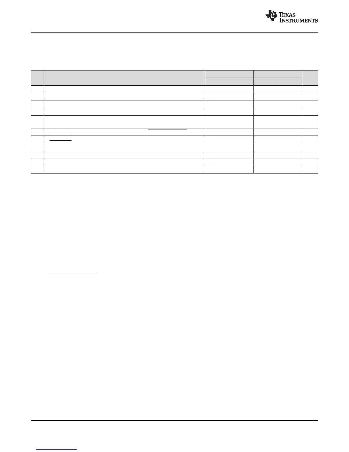
6.24.2 LCD Raster Mode
Table 6-110. Switching Characteristics Over Recommended Operating Conditions for LCD Raster Mode
See Figure 6-62 through Figure 6-66
NO. PARAMETER
1.3V, 1.2V, 1.1V 1.0V
UNIT
MIN MAX MIN MAX
1 t
c(PIXEL_CLK)
Cycle time, pixel clock 26.66 33.33 ns
2 t
w(PIXEL_CLK_H)
Pulse duration, pixel clock high 10 10 ns
3 t
w(PIXEL_CLK_L)
Pulse duration, pixel clock low 10 10 ns
4 t
d(LCD_D_V)
Delay time, LCD_PCLK high to LCD_D[15:0] valid (write) 0 7 0 9 ns
5 t
d(LCD_D_IV)
Delay time, LCD_PCLK high to LCD_D[15:0] invalid
(write)
0 7 0 9 ns
6 t
d(LCD_AC_ENB_CS_A)
Delay time, LCD_PCLK low to LCD_AC_ENB_CS high 0 7 0 9 ns
7 t
d(LCD_AC_ENB_CS_I)
Delay time, LCD_PCLK low to LCD_AC_ENB_CS low 0 7 0 9 ns
8 t
d(LCD_VSYNC_A)
Delay time, LCD_PCLK low to LCD_VSYNC high 0 7 0 9 ns
9 t
d(LCD_VSYNC_I)
Delay time, LCD_PCLK low to LCD_VSYNC low 0 7 0 9 ns
10 t
d(LCD_HSYNC_A)
Delay time, LCD_PCLK high to LCD_HSYNC high 0 7 0 9 ns
11 t
d(LCD_HSYNC_I)
Delay time, LCD_PCLK high to LCD_HSYNC low 0 7 0 9 ns
Frame-to-frame timing is derived through the following parameters in the LCD (RASTER_TIMING_1)
register:
• Vertical front porch (VFP)
• Vertical sync pulse width (VSW)
• Vertical back porch (VBP)
• Lines per panel (LPP)
Line-to-line timing is derived through the following parameters in the LCD (RASTER_TIMING_0) register:
• Horizontal front porch (HFP)
• Horizontal sync pulse width (HSW)
• Horizontal back porch (HBP)
• Pixels per panel (PPL)
LCD_AC_ENB_CS timing is derived through the following parameter in the LCD (RASTER_TIMING_2)
register:
• AC bias frequency (ACB)
The display format produced in raster mode is shown in Figure 6-62. An entire frame is delivered one line
at a time. The first line delivered starts at data pixel (1, 1) and ends at data pixel (P, 1). The last line
delivered starts at data pixel (1, L) and ends at data pixel (P, L). The beginning of each new frame is
denoted by the activation of I/O signal LCD_VSYNC. The beginning of each new line is denoted by the
activation of I/O signal LCD_HSYNC.
 Loading...


