VP_CLKOUTx
(PositiveEdge
Clocking)
VP_CLKOUTx
(NegativeEdge
Clocking)
VP_DOUTx
1
2
11 12
44
3
VP_CLKIN0/1
VP_DINx/FIELD/
HSYNC/VSYNC
1
2
238
TMS320C6748
SPRS590G –JUNE 2009–REVISED JANUARY 2017
www.ti.com
Submit Documentation Feedback
Product Folder Links: TMS320C6748
Peripheral Information and Electrical Specifications Copyright © 2009–2017, Texas Instruments Incorporated
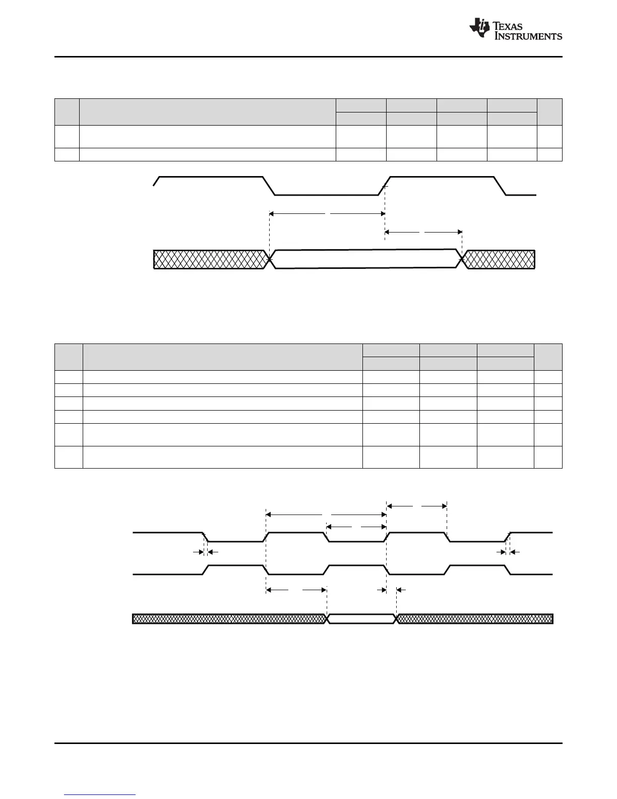
Table 6-120. Timing Requirements for VPIF Channels 0/1 Video Capture Data and Control Inputs
(see Figure 6-76)
NO.
1.3V 1.2V 1.1V 1.0V
UNIT
MIN MAX MIN MAX MIN MAX MIN MAX
1
t
su(VDINV-
VKIH)
Setup time, VP_DINx valid before VP_OSCIN0/1 high 4 4 6 7 ns
2 t
h(VKIH-VDINV)
Hold time, VP_DINx valid after VP_CLKIN0/1 high 0.5 0 0 0 ns
(1) C = VP_CLKO2/3 period in ns.
Figure 6-76. VPIF Channels 0/1 Video Capture Data and Control Input Timing
Table 6-121. Switching Characteristics Over Recommended Operating Conditions for Video Data Shown
With Respect to VP_CLKOUT2/3
(1)
(see Figure 6-77)
NO. PARAMETER
1.3V, 1.2V 1.1V 1.0V
UNIT
MIN MAX MIN MAX MIN MAX
1 t
c(VKO)
Cycle time, VP_CLKOUT2/3 13.3 20 37 ns
2 t
w(VKOH)
Pulse duration, VP_CLKOUT2/3 high 0.4C 0.4C 0.4C ns
3 t
w(VKOL)
Pulse duration, VP_CLKOUT2/3 low 0.4C 0.4C 0.4C ns
4 t
t(VKO)
Transition time, VP_CLKOUT2/3 5 5 5 ns
11 t
d(VKOH-VPDOUTV)
Delay time,
VP_CLKOUT2/3 high to VP_DOUTx valid
8.5 12 17 ns
12 t
d(VCLKOH-VPDOUTIV)
Delay time,
VP_CLKOUT2/3 high to VP_DOUTx invalid
1.5 1.5 1.5 ns
Figure 6-77. VPIF Channels 2/3 Video Display Data Output Timing With Respect to VP_CLKOUT2/3
 Loading...


