TCK
TDO
TDI/TMS/TRST
1
6
6
5
4
3
2
262
TMS320C6748
SPRS590G –JUNE 2009–REVISED JANUARY 2017
www.ti.com
Submit Documentation Feedback
Product Folder Links: TMS320C6748
Peripheral Information and Electrical Specifications Copyright © 2009–2017, Texas Instruments Incorporated
6.34.4.2 JTAG Test-Port Electrical Data/Timing
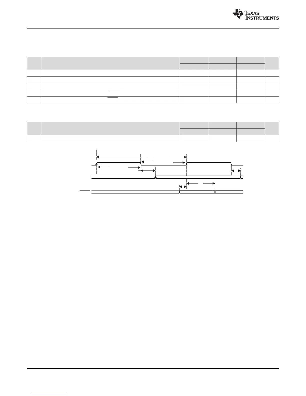
Table 6-147. Timing Requirements for JTAG Test Port (see Figure 6-89)
No.
1.3V, 1.2V 1.1V 1.0V
UNIT
MIN MAX MIN MAX MIN MAX
1 t
c(TCK)
Cycle time, TCK 40 50 66.6 ns
2 t
w(TCKH)
Pulse duration, TCK high 16 20 26.6 ns
3 t
w(TCKL)
Pulse duration, TCK low 16 20 26.6 ns
4 t
su(TDIV-TCKH)
Setup time, TDI/TMS/TRST valid before TCK high 4 4 4 ns
5 t
h(TCLKH-TDIV)
Hold time, TDI/TMS/TRST valid after TCK high 4 6 8 ns
Table 6-148. Switching Characteristics Over Recommended Operating Conditions for JTAG Test Port
(see Figure 6-89)
No. PARAMETER
1.3V, 1.2V 1.1V 1.0V
UNIT
MIN MAX MIN MAX MIN MAX
6 t
d(TCKL-TDOV)
Delay time, TCK low to TDO valid 18 23 31 ns
Figure 6-89. JTAG Test-Port Timing
6.34.5 JTAG 1149.1 Boundary Scan Considerations
To use boundary scan, the following sequence should be followed:
• Execute a valid reset sequence and exit reset
• Wait at least 6000 OSCIN clock cycles
• Enter boundary scan mode using the JTAG pins
No specific value is required on the EMU0 and EMU1 pins for boundary scan testing. If TRST is not driven
by the boundary scan tool or tester, TRST should be externally pulled high during boundary scan testing.