77
TMS320C6748
www.ti.com
SPRS590G –JUNE 2009–REVISED JANUARY 2017
Submit Documentation Feedback
Product Folder Links: TMS320C6748
SpecificationsCopyright © 2009–2017, Texas Instruments Incorporated
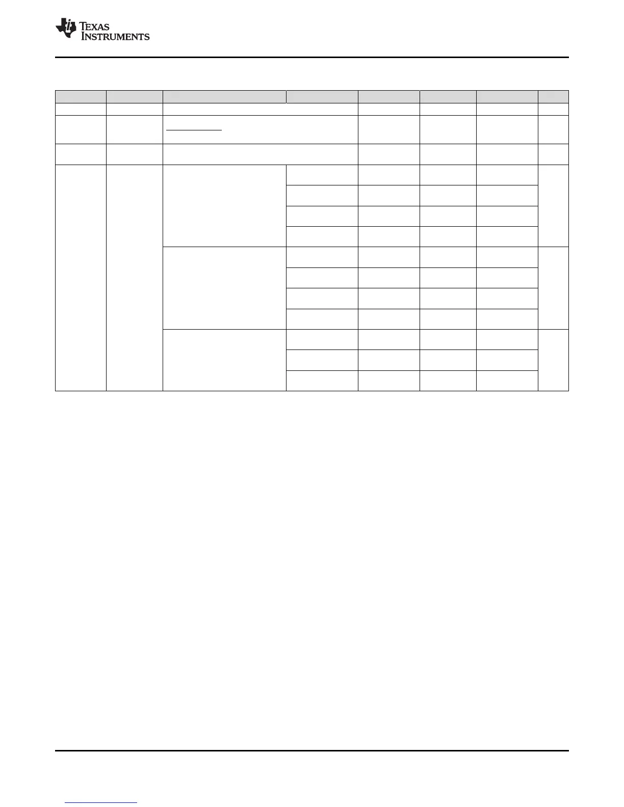
Recommended Operating Conditions (continued)
NAME DESCRIPTION CONDITION MIN NOM MAX UNIT
(5) Whichever is smaller. P = the period of the applied signal. Maintaining transition times as fast as possible is recommended to improve
noise immunity on input signals.
(6) This operating point is not supported on revision 1.x silicon.
(7) This operating point is 300 MHz on revision 1.x silicon.
USB USB0_VBUS USB external charge pump input 0 5.25 V
Differential
Clock Input
Voltage
Differential input voltage, SATA_REFCLKP and
SATA_REFCLKN
250 2000 mV
Transition
Time
t
t
Transition time, 10%-90%, All Inputs (unless otherwise
specified in the electrical data sections)
0.25P or 10
(5)
ns
Operating
Frequency
F
PLL0_SYSCLK1,6
Commercial temperature grade
(default)
CVDD = 1.3V
operating point
0 456
(6)
MHz
CVDD = 1.2V
operating point
0 375
(7)
CVDD = 1.1V
operating point
0 200
(6)
CVDD = 1.0V
operating point
0 100
(6)
Industrial temperature grade
(D suffix)
CVDD = 1.3V
operating point
0 456
(6)
MHz
CVDD = 1.2V
operating point
0 375
(7)
CVDD = 1.1V
operating point
0 200
(6)
CVDD = 1.0V
operating point
0 100
(6)
Extended temperature grade
(A suffix)
CVDD = 1.2V
operating point
0 375
(7)
MHz
CVDD = 1.1V
operating point
0 200
(6)
CVDD = 1.0V
operating point
0 100
(6)